


*** INCOMPLETE ***
The invention of the bipolar transistor in 1948 ushered in a revolution in electronics. Technical feats previously requiring relatively large, mechanically fragile, power-hungry vacuum tubes were suddenly achievable with tiny, mechanically rugged, power-thrifty specks of crystalline silicon. This revolution made possible the design and manufacture of lightweight, inexpensive electronic devices that we now take for granted. Understanding how transistors function is of paramount importance to anyone interested in understanding modern electronics.
My intent here is to focus as exclusively as possible on the practical function and application of bipolar transistors, rather than to explore the quantum world of semiconductor theory. Discussions of holes and electrons are better left to another chapter in my opinion. Here I want to explore how to use these components, not analyze their intimate internal details. I don't mean to downplay the importance of understanding semiconductor physics, but sometimes an intense focus on solid-state physics detracts from understanding these devices' functions on a component level. In taking this approach, however, I assume that the reader possesses a certain minimum knowledge of semiconductors: the difference between "P" and "N" doped semiconductors, the functional characteristics of a PN (diode) junction, and the meanings of the terms "reverse biased" and "forward biased." If these concepts are unclear to you, it is best to refer to earlier chapters in this book before proceeding with this one.
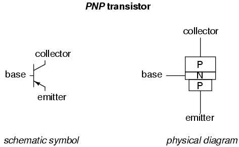
A bipolar transistor consists of a three-layer "sandwich" of doped (extrinsic) semiconductor materials, either P-N-P or N-P-N. Each layer forming the transistor has a specific name, and each layer is provided with a wire contact for connection to a circuit. Shown here are schematic symbols and physical diagrams of these two transistor types:
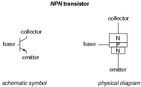
The only functional difference between a PNP transistor and an NPN transistor is the proper biasing (polarity) of the junctions when operating. For any given state of operation, the current directions and voltage polarities for each type of transistor are exactly opposite each other.
Bipolar transistors work as current-controlled current regulators. In other words, they restrict the amount of current that can go through them according to a smaller, controlling current. The main current that is controlled goes from collector to emitter, or from emitter to collector, depending on the type of transistor it is (PNP or NPN, respectively). The small current that controls the main current goes from base to emitter, or from emitter to base, once again depending on the type of transistor it is (PNP or NPN, respectively). According to the confusing standards of semiconductor symbology, the arrow always points against the direction of electron flow:
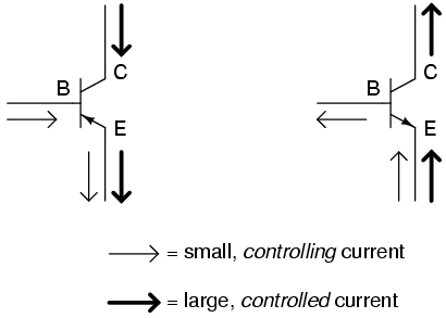
Bipolar transistors are called bipolar because the main flow of electrons through them takes place in two types of semiconductor material: P and N, as the main current goes from emitter to collector (or visa-versa). In other words, two types of charge carriers -- electrons and holes -- comprise this main current through the transistor.
As you can see, the controlling current and the controlled current always mesh together through the emitter wire, and their electrons always flow against the direction of the transistor's arrow. This is the first and foremost rule in the use of transistors: all currents must be going in the proper directions for the device to work as a current regulator. The small, controlling current is usually referred to simply as the base current because it is the only current that goes through the base wire of the transistor. Conversely, the large, controlled current is referred to as the collector current because it is the only current that goes through the collector wire. The emitter current is the sum of the base and collector currents, in compliance with Kirchhoff's Current Law.
If there is no current through the base of the transistor, it shuts off like an open switch and prevents current through the collector. If there is a base current, then the transistor turns on like a closed switch and allows a proportional amount of current through the collector. Collector current is primarily limited by the base current, regardless of the amount of voltage available to push it. The next section will explore in more detail the use of bipolar transistors as switching elements.
Because a transistor's collector current is proportionally limited by its base current, it can be used as a sort of current-controlled switch. A relatively small flow of electrons sent through the base of the transistor has the ability to exert control over a much larger flow of electrons through the collector.
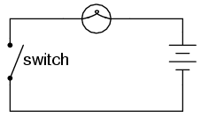
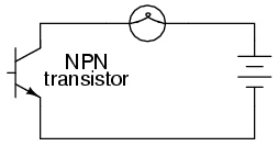
Suppose we had a lamp that we wanted to turn on and off by means of a switch. Such a circuit would be extremely simple:
For the sake of illustration, let's insert a transistor in place of the switch to show how it can control the flow of electrons through the lamp. Remember that the controlled current through a transistor must go between collector and emitter. Since it's the current through the lamp that we want to control, we must position the collector and emitter of our transistor where the two contacts of the switch are now. We must also make sure that the lamp's current will move against the direction of the emitter arrow symbol to ensure that the transistor's junction bias will be correct:
In this example I happened to choose an NPN transistor. A PNP transistor could also have been chosen for the job, and its application would look like this:
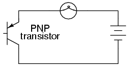
The choice between NPN and PNP is really arbitrary. All that matters is that the proper current directions are maintained for the sake of correct junction biasing (electron flow going against the transistor symbol's arrow).
Going back to the NPN transistor in our example circuit, we are faced with the need to add something more so that we can have base current. Without a connection to the base wire of the transistor, base current will be zero, and the transistor cannot turn on, resulting in a lamp that is always off. Remember that for an NPN transistor, base current must consist of electrons flowing from emitter to base (against the emitter arrow symbol, just like the lamp current). Perhaps the simplest thing to do would be to connect a switch between the base and collector wires of the transistor like this:
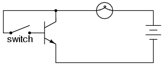
If the switch is open, the base wire of the transistor will be left "floating" (not connected to anything) and there will be no current through it. In this state, the transistor is said to be cutoff. If the switch is closed, however, electrons will be able to flow from the emitter through to the base of the transistor, through the switch and up to the left side of the lamp, back to the positive side of the battery. This base current will enable a much larger flow of electrons from the emitter through to the collector, thus lighting up the lamp. In this state of maximum circuit current, the transistor is said to be saturated.
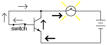
Of course, it may seem pointless to use a transistor in this capacity to control the lamp. After all, we're still using a switch in the circuit, aren't we? If we're still using a switch to control the lamp -- if only indirectly -- then what's the point of having a transistor to control the current? Why not just go back to our original circuit and use the switch directly to control the lamp current?
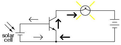
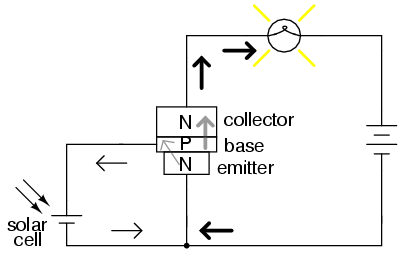
There are a couple of points to be made here, actually. First is the fact that when used in this manner, the switch contacts need only handle what little base current is necessary to turn the transistor on, while the transistor itself handles the majority of the lamp's current. This may be an important advantage if the switch has a low current rating: a small switch may be used to control a relatively high-current load. Perhaps more importantly, though, is the fact that the current-controlling behavior of the transistor enables us to use something completely different to turn the lamp on or off. Consider this example, where a solar cell is used to control the transistor, which in turn controls the lamp:
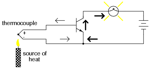
Or, we could use a thermocouple to provide the necessary base current to turn the transistor on:
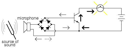
Even a microphone of sufficient voltage and current output could be used to turn the transistor on, provided its output is rectified from AC to DC so that the emitter-base PN junction within the transistor will always be forward-biased:
The point should be quite apparent by now: any sufficient source of DC current may be used to turn the transistor on, and that source of current need only be a fraction of the amount of current needed to energize the lamp. Here we see the transistor functioning not only as a switch, but as a true amplifier: using a relatively low-power signal to control a relatively large amount of power. Please note that the actual power for lighting up the lamp comes from the battery to the right of the schematic. It is not as though the small signal current from the solar cell, thermocouple, or microphone is being magically transformed into a greater amount of power. Rather, those small power sources are simply controlling the battery's power to light up the lamp.
Bipolar transistors are constructed of a three-layer semiconductor "sandwich," either PNP or NPN. As such, they register as two diodes connected back-to-back when tested with a multimeter's "resistance" or "diode check" functions:
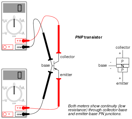
Here I'm assuming the use of a multimeter with only a single continuity range (resistance) function to check the PN junctions. Some multimeters are equipped with two separate continuity check functions: resistance and "diode check," each with its own purpose. If your meter has a designated "diode check" function, use that rather than the "resistance" range, and the meter will display the actual forward voltage of the PN junction and not just whether or not it conducts current.
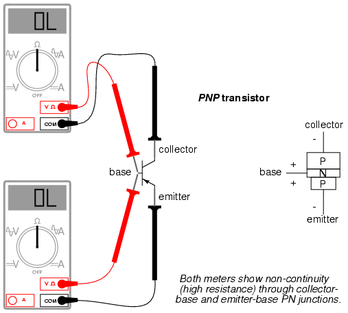
Meter readings will be exactly opposite, of course, for an NPN transistor, with both PN junctions facing the other way. If a multimeter with a "diode check" function is used in this test, it will be found that the emitter-base junction possesses a slightly greater forward voltage drop than the collector-base junction. This forward voltage difference is due to the disparity in doping concentration between the emitter and collector regions of the transistor: the emitter is a much more heavily doped piece of semiconductor material than the collector, causing its junction with the base to produce a higher forward voltage drop.
Knowing this, it becomes possible to determine which wire is which on an unmarked transistor. This is important because transistor packaging, unfortunately, is not standardized. All bipolar transistors have three wires, of course, but the positions of the three wires on the actual physical package are not arranged in any universal, standardized order.
Suppose a technician finds a bipolar transistor and proceeds to measure continuity with a multimeter set in the "diode check" mode. Measuring between pairs of wires and recording the values displayed by the meter, the technician obtains the following data:
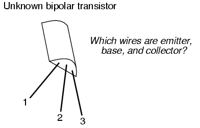
The only combinations of test points giving conducting meter readings are wires 1 and 3 (red test lead on 1 and black test lead on 3), and wires 2 and 3 (red test lead on 2 and black test lead on 3). These two readings must indicate forward biasing of the emitter-to-base junction (0.655 volts) and the collector-to-base junction (0.621 volts).
Now we look for the one wire common to both sets of conductive readings. It must be the base connection of the transistor, because the base is the only layer of the three-layer device common to both sets of PN junctions (emitter-base and collector-base). In this example, that wire is number 3, being common to both the 1-3 and the 2-3 test point combinations. In both those sets of meter readings, the black (-) meter test lead was touching wire 3, which tells us that the base of this transistor is made of N-type semiconductor material (black = negative). Thus, the transistor is an PNP type with base on wire 3, emitter on wire 1 and collector on wire 2:
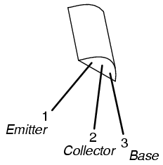
Please note that the base wire in this example is not the middle lead of the transistor, as one might expect from the three-layer "sandwich" model of a bipolar transistor. This is quite often the case, and tends to confuse new students of electronics. The only way to be sure which lead is which is by a meter check, or by referencing the manufacturer's "data sheet" documentation on that particular part number of transistor.
Knowing that a bipolar transistor behaves as two back-to-back diodes when tested with a conductivity meter is helpful for identifying an unknown transistor purely by meter readings. It is also helpful for a quick functional check of the transistor. If the technician were to measure continuity in any more than two or any less than two of the six test lead combinations, he or she would immediately know that the transistor was defective (or else that it wasn't a bipolar transistor but rather something else -- a distinct possibility if no part numbers can be referenced for sure identification!). However, the "two diode" model of the transistor fails to explain how or why it acts as an amplifying device.
To better illustrate this paradox, let's examine one of the transistor switch circuits using the physical diagram rather than the schematic symbol to represent the transistor. This way the two PN junctions will be easier to see:
A grey-colored diagonal arrow shows the direction of electron flow through the emitter-base junction. This part makes sense, since the electrons are flowing from the N-type emitter to the P-type base: the junction is obviously forward-biased. However, the base-collector junction is another matter entirely. Notice how the grey-colored thick arrow is pointing in the direction of electron flow (upwards) from base to collector. With the base made of P-type material and the collector of N-type material, this direction of electron flow is clearly backwards to the direction normally associated with a PN junction! A normal PN junction wouldn't permit this "backward" direction of flow, at least not without offering significant opposition. However, when the transistor is saturated, there is very little opposition to electrons all the way from emitter to collector, as evidenced by the lamp's illumination!
Clearly then, something is going on here that defies the simple "two-diode" explanatory model of the bipolar transistor. When I was first learning about transistor operation, I tried to construct my own transistor from two back-to-back diodes, like this:
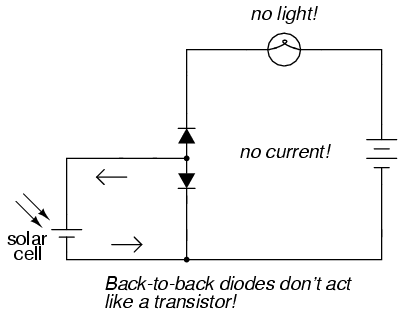
My circuit didn't work, and I was mystified. However useful the "two diode" description of a transistor might be for testing purposes, it doesn't explain how a transistor can behave as a controlled switch.
What happens in a transistor is this: the reverse bias of the base-collector junction prevents collector current when the transistor is in cutoff mode (that is, when there is no base current). However, when the base-emitter junction is forward biased by the controlling signal, the normally-blocking action of the base-collector junction is overridden and current is permitted through the collector, despite the fact that electrons are going the "wrong way" through that PN junction. This action is dependent on the quantum physics of semiconductor junctions, and can only take place when the two junctions are properly spaced and the doping concentrations of the three layers are properly proportioned. Two diodes wired in series fail to meet these criteria, and so the top diode can never "turn on" when it is reversed biased, no matter how much current goes through the bottom diode in the base wire loop.
That doping concentrations play a crucial part in the special abilities of the transistor is further evidenced by the fact that collector and emitter are not interchangeable. If the transistor is merely viewed as two back-to-back PN junctions, or merely as a plain N-P-N or P-N-P sandwich of materials, it may seem as though either end of the transistor could serve as collector or emitter. This, however, is not true. If connected "backwards" in a circuit, a base-collector current will fail to control current between collector and emitter. Despite the fact that both the emitter and collector layers of a bipolar transistor are of the same doping type (either N or P), they are definitely not identical!
So, current through the emitter-base junction allows current through the reverse-biased base-collector junction. The action of base current can be thought of as "opening a gate" for current through the collector. More specifically, any given amount of emitter-to-base current permits a limited amount of base-to-collector current. For every electron that passes through the emitter-base junction and on through the base wire, there is allowed a certain, restricted number of electrons to pass through the base-collector junction and no more.
In the next section, this current-limiting behavior of the transistor will be investigated in more detail.
When a transistor is in the fully-off state (like an open switch), it is said to be cutoff. Conversely, when it is fully conductive between emitter and collector (passing as much current through the collector as the collector power supply and load will allow), it is said to be saturated. These are the two modes of operation explored thus far in using the transistor as a switch.
However, bipolar transistors don't have to be restricted to these two extreme modes of operation. As we learned in the previous section, base current "opens a gate" for a limited amount of current through the collector. If this limit for the controlled current is greater than zero but less than the maximum allowed by the power supply and load circuit, the transistor will "throttle" the collector current in a mode somewhere between cutoff and saturation. This mode of operation is called the active mode.
An automotive analogy for transistor operation is as follows: cutoff is the condition where there is no motive force generated by the mechanical parts of the car to make it move. In cutoff mode, the brake is engaged (zero base current), preventing motion (collector current). Active mode is when the automobile is cruising at a constant, controlled speed (constant, controlled collector current) as dictated by the driver. Saturation is when the automobile is driving up a steep hill that prevents it from going as fast as the driver would wish. In other words, a "saturated" automobile is one where the accelerator pedal is pushed all the way down (base current calling for more collector current than can be provided by the power supply/load circuit).
I'll set up a circuit for SPICE simulation to demonstrate what happens when a transistor is in its active mode of operation:
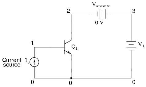
"Q" is the standard letter designation for a transistor in a schematic diagram, just as "R" is for resistor and "C" is for capacitor. In this circuit, we have an NPN transistor powered by a battery (V1) and controlled by current through a current source (I1). A current source is a device that outputs a specific amount of current, generating as much or as little voltage as necessary across its terminals to ensure that exact amount of current through it. Current sources are notoriously difficult to find in nature (unlike voltage sources, which by contrast attempt to maintain a constant voltage, outputting as much or as little current in the fulfillment of that task), but can be simulated with a small collection of electronic components. As we are about to see, transistors themselves tend to mimic the constant-current behavior of a current source in their ability to regulate current at a fixed value.
In the SPICE simulation, I'll set the current source at a constant value of 20 µA, then vary the voltage source (V1) over a range of 0 to 2 volts and monitor how much current goes through it. The "dummy" battery (Vammeter) with its output of 0 volts serves merely to provide SPICE with a circuit element for current measurement.
bipolar transistor simulation
i1 0 1 dc 20u
q1 2 1 0 mod1
vammeter 3 2 dc 0
v1 3 0 dc
.model mod1 npn
.dc v1 0 2 0.05
.plot dc i(vammeter)
.end
type        npn
is        1.00E-16
bf         100.000
nf           1.000
br           1.000
nr           1.000
v1      i(ammeter) -1.000E-03   0.000E+00   1.000E-03    2.000E-03
- - - - - - - - - - - - - - - - - - - - - - - - - - - - - - - - -
0.000E+00 -1.980E-05 .             *             .             .
5.000E-02  9.188E-05 .             .*            .             .
1.000E-01  6.195E-04 .             .        *    .             .
1.500E-01  1.526E-03 .             .             .      *      .
2.000E-01  1.914E-03 .             .             .            *.
2.500E-01  1.987E-03 .             .             .             *
3.000E-01  1.998E-03 .             .             .             *
3.500E-01  2.000E-03 .             .             .             *
4.000E-01  2.000E-03 .             .             .             *
4.500E-01  2.000E-03 .             .             .             *
5.000E-01  2.000E-03 .             .             .             *
5.500E-01  2.000E-03 .             .             .             *
6.000E-01  2.000E-03 .             .             .             *
6.500E-01  2.000E-03 .             .             .             *
7.000E-01  2.000E-03 .             .             .             *
7.500E-01  2.000E-03 .             .             .             *
8.000E-01  2.000E-03 .             .             .             *
8.500E-01  2.000E-03 .             .             .             *
9.000E-01  2.000E-03 .             .             .             *
9.500E-01  2.000E-03 .             .             .             *
1.000E+00  2.000E-03 .             .             .             *
1.050E+00  2.000E-03 .             .             .             *
1.100E+00  2.000E-03 .             .             .             *
1.150E+00  2.000E-03 .             .             .             *
1.200E+00  2.000E-03 .             .             .             *
1.250E+00  2.000E-03 .             .             .             *
1.300E+00  2.000E-03 .             .             .             *
1.350E+00  2.000E-03 .             .             .             *
1.400E+00  2.000E-03 .             .             .             *
1.450E+00  2.000E-03 .             .             .             *
1.500E+00  2.000E-03 .             .             .             *
1.550E+00  2.000E-03 .             .             .             *
1.600E+00  2.000E-03 .             .             .             *
1.650E+00  2.000E-03 .             .             .             *
1.700E+00  2.000E-03 .             .             .             *
1.750E+00  2.000E-03 .             .             .             *
1.800E+00  2.000E-03 .             .             .             *
1.850E+00  2.000E-03 .             .             .             *
1.900E+00  2.000E-03 .             .             .             *
1.950E+00  2.000E-03 .             .             .             *
2.000E+00  2.000E-03 .             .             .             *
- - - - - - - - - - - - - - - - - - - - - - - - - - - - - - - - -
The constant base current of 20 µA sets a collector current limit of 2 mA, exactly 100 times as much. Notice how flat the curve is for collector current over the range of battery voltage from 0 to 2 volts. The only exception to this featureless plot is at the very beginning, where the battery increases from 0 volts to 0.25 volts. There, the collector current increases rapidly from 0 amps to its limit of 2 mA.
Let's see what happens if we vary the battery voltage over a wider range, this time from 0 to 50 volts. We'll keep the base current steady at 20 µA:
bipolar transistor simulation
i1 0 1 dc 20u
q1 2 1 0 mod1
vammeter 3 2 dc 0
v1 3 0 dc
.model mod1 npn
.dc v1 0 50 2
.plot dc i(vammeter)
.end
type        npn
is        1.00E-16
bf         100.000
nf           1.000
br           1.000
nr           1.000
v1      i(ammeter) -1.000E-03   0.000E+00   1.000E-03    2.000E-03
- - - - - - - - - - - - - - - - - - - - - - - - - - - - - - - - -
0.000E+00 -1.980E-05 .             *             .             .
2.000E+00  2.000E-03 .             .             .             *
4.000E+00  2.000E-03 .             .             .             *
6.000E+00  2.000E-03 .             .             .             *
8.000E+00  2.000E-03 .             .             .             *
1.000E+01  2.000E-03 .             .             .             *
1.200E+01  2.000E-03 .             .             .             *
1.400E+01  2.000E-03 .             .             .             *
1.600E+01  2.000E-03 .             .             .             *
1.800E+01  2.000E-03 .             .             .             *
2.000E+01  2.000E-03 .             .             .             *
2.200E+01  2.000E-03 .             .             .             *
2.400E+01  2.000E-03 .             .             .             *
2.600E+01  2.000E-03 .             .             .             *
2.800E+01  2.000E-03 .             .             .             *
3.000E+01  2.000E-03 .             .             .             *
3.200E+01  2.000E-03 .             .             .             *
3.400E+01  2.000E-03 .             .             .             *
3.600E+01  2.000E-03 .             .             .             *
3.800E+01  2.000E-03 .             .             .             *
4.000E+01  2.000E-03 .             .             .             *
4.200E+01  2.000E-03 .             .             .             *
4.400E+01  2.000E-03 .             .             .             *
4.600E+01  2.000E-03 .             .             .             *
4.800E+01  2.000E-03 .             .             .             *
5.000E+01  2.000E-03 .             .             .             *
- - - - - - - - - - - - - - - - - - - - - - - - - - - - - - - - -
Same result! The collector current holds absolutely steady at 2 mA despite the fact that the battery (v1) voltage varies all the way from 0 to 50 volts. It would appear from our simulation that collector-to-emitter voltage has little effect over collector current, except at very low levels (just above 0 volts). The transistor is acting as a current regulator, allowing exactly 2 mA through the collector and no more.
Now let's see what happens if we increase the controlling (I1) current from 20 µA to 75 µA, once again sweeping the battery (V1) voltage from 0 to 50 volts and graphing the collector current:
bipolar transistor simulation
i1 0 1 dc 75u
q1 2 1 0 mod1
vammeter 3 2 dc 0
v1 3 0 dc
.model mod1 npn
.dc v1 0 50 2
.plot dc i(vammeter)
.end
type        npn
is        1.00E-16
bf         100.000
nf           1.000
br           1.000
nr           1.000
v1      i(ammeter) -5.000E-03   0.000E+00    5.000E-03    1.000E-02
- - - - - - - - - - - - - - - - - - - - - - - - - - - - - - - - -
0.000E+00 -7.426E-05 .             *             .             .
2.000E+00  7.500E-03 .             .             .      *      .
4.000E+00  7.500E-03 .             .             .      *      .
6.000E+00  7.500E-03 .             .             .      *      .
8.000E+00  7.500E-03 .             .             .      *      .
1.000E+01  7.500E-03 .             .             .      *      .
1.200E+01  7.500E-03 .             .             .      *      .
1.400E+01  7.500E-03 .             .             .      *      .
1.600E+01  7.500E-03 .             .             .      *      .
1.800E+01  7.500E-03 .             .             .      *      .
2.000E+01  7.500E-03 .             .             .      *      .
2.200E+01  7.500E-03 .             .             .      *      .
2.400E+01  7.500E-03 .             .             .      *      .
2.600E+01  7.500E-03 .             .             .      *      .
2.800E+01  7.500E-03 .             .             .      *      .
3.000E+01  7.500E-03 .             .             .      *      .
3.200E+01  7.500E-03 .             .             .      *      .
3.400E+01  7.500E-03 .             .             .      *      .
3.600E+01  7.500E-03 .             .             .      *      .
3.800E+01  7.500E-03 .             .             .      *      .
4.000E+01  7.500E-03 .             .             .      *      .
4.200E+01  7.500E-03 .             .             .      *      .
4.400E+01  7.500E-03 .             .             .      *      .
4.600E+01  7.500E-03 .             .             .      *      .
4.800E+01  7.500E-03 .             .             .      *      .
5.000E+01  7.500E-03 .             .             .      *      .
- - - - - - - - - - - - - - - - - - - - - - - - - - - - - - - - -
Not surprisingly, SPICE gives us a similar plot: a flat line, holding steady this time at 7.5 mA -- exactly 100 times the base current -- over the range of battery voltages from just above 0 volts to 50 volts. It appears that the base current is the deciding factor for collector current, the V1 battery voltage being irrelevant so long as it's above a certain minimum level.
This voltage/current relationship is entirely different from what we're used to seeing across a resistor. With a resistor, current increases linearly as the voltage across it increases. Here, with a transistor, current from emitter to collector stays limited at a fixed, maximum value no matter how high the voltage across emitter and collector increases.
Often it is useful to superimpose several collector current/voltage graphs for different base currents on the same graph. A collection of curves like this -- one curve plotted for each distinct level of base current -- for a particular transistor is called the transistor's characteristic curves:
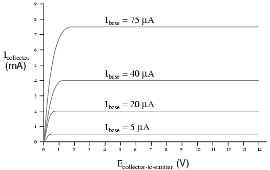
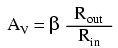
Each curve on the graph reflects the collector current of the transistor, plotted over a range of collector-to-emitter voltages, for a given amount of base current. Since a transistor tends to act as a current regulator, limiting collector current to a proportion set by the base current, it is useful to express this proportion as a standard transistor performance measure. Specifically, the ratio of collector current to base current is known as the Beta ratio (symbolized by the Greek letter β):
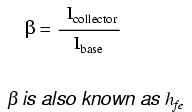
Sometimes the β ratio is designated as "hfe," a label used in a branch of mathematical semiconductor analysis known as "hybrid parameters" which strives to achieve very precise predictions of transistor performance with detailed equations. Hybrid parameter variables are many, but they are all labeled with the general letter "h" and a specific subscript. The variable "hfe" is just another (standardized) way of expressing the ratio of collector current to base current, and is interchangeable with "β." Like all ratios, β is unitless.
β for any transistor is determined by its design: it cannot be altered after manufacture. However, there are so many physical variables impacting β that it is rare to have two transistors of the same design exactly match. If a circuit design relies on equal β ratios between multiple transistors, "matched sets" of transistors may be purchased at extra cost. However, it is generally considered bad design practice to engineer circuits with such dependencies.
It would be nice if the β of a transistor remained stable for all operating conditions, but this is not true in real life. For an actual transistor, the β ratio may vary by a factor of over 3 within its operating current limits. For example, a transistor with advertised β of 50 may actually test with Ic/Ib ratios as low as 30 and as high as 100, depending on the amount of collector current, the transistor's temperature, and frequency of amplified signal, among other factors. For tutorial purposes it is adequate to assume a constant β for any given transistor (which is what SPICE tends to do in a simulation), but just realize that real life is not that simple!
Sometimes it is helpful for comprehension to "model" complex electronic components with a collection of simpler, better-understood components. The following is a popular model shown in many introductory electronics texts:
This model casts the transistor as a combination of diode and rheostat (variable resistor). Current through the base-emitter diode controls the resistance of the collector-emitter rheostat (as implied by the dashed line connecting the two components), thus controlling collector current. An NPN transistor is modeled in the figure shown, but a PNP transistor would be only slightly different (only the base-emitter diode would be reversed). This model succeeds in illustrating the basic concept of transistor amplification: how the base current signal can exert control over the collector current. However, I personally don't like this model because it tends to miscommunicate the notion of a set amount of collector-emitter resistance for a given amount of base current. If this were true, the transistor wouldn't regulate collector current at all like the characteristic curves show. Instead of the collector current curves flattening out after their brief rise as the collector-emitter voltage increases, the collector current would be directly proportional to collector-emitter voltage, rising steadily in a straight line on the graph.
A better transistor model, often seen in more advanced textbooks, is this:
It casts the transistor as a combination of diode and current source, the output of the current source being set at a multiple (β ratio) of the base current. This model is far more accurate in depicting the true input/output characteristics of a transistor: base current establishes a certain amount of collector current, rather than a certain amount of collector-emitter resistance as the first model implies. Also, this model is favored when performing network analysis on transistor circuits, the current source being a well-understood theoretical component. Unfortunately, using a current source to model the transistor's current-controlling behavior can be misleading: in no way will the transistor ever act as a source of electrical energy, which the current source symbol implies is a possibility.
My own personal suggestion for a transistor model substitutes a constant-current diode for the current source:
Since no diode ever acts as a source of electrical energy, this analogy escapes the false implication of the current source model as a source of power, while depicting the transistor's constant-current behavior better than the rheostat model. Another way to describe the constant-current diode's action would be to refer to it as a current regulator, so this transistor illustration of mine might also be described as a diode-current regulator model. The greatest disadvantage I see to this model is the relative obscurity of constant-current diodes. Many people may be unfamiliar with their symbology or even of their existence, unlike either rheostats or current sources, which are commonly known.
At the beginning of this chapter we saw how transistors could be used as switches, operating in either their "saturation" or "cutoff" modes. In the last section we saw how transistors behave within their "active" modes, between the far limits of saturation and cutoff. Because transistors are able to control current in an analog (infinitely divisible) fashion, they find use as amplifiers for analog signals.
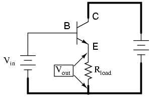
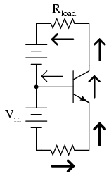
One of the simpler transistor amplifier circuits to study is the one used previously for illustrating the transistor's switching ability:
It is called the common-emitter configuration because (ignoring the power supply battery) both the signal source and the load share the emitter lead as a common connection point. This is not the only way in which a transistor may be used as an amplifier, as we will see in later sections of this chapter:
Before, this circuit was shown to illustrate how a relatively small current from a solar cell could be used to saturate a transistor, resulting in the illumination of a lamp. Knowing now that transistors are able to "throttle" their collector currents according to the amount of base current supplied by an input signal source, we should be able to see that the brightness of the lamp in this circuit is controllable by the solar cell's light exposure. When there is just a little light shone on the solar cell, the lamp will glow dimly. The lamp's brightness will steadily increase as more light falls on the solar cell.
Suppose that we were interested in using the solar cell as a light intensity instrument. We want to be able to measure the intensity of incident light with the solar cell by using its output current to drive a meter movement. It is possible to directly connect a meter movement to a solar cell for this purpose. In fact, the simplest light-exposure meters for photography work are designed like this:
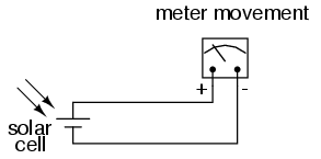
While this approach might work for moderate light intensity measurements, it would not work as well for low light intensity measurements. Because the solar cell has to supply the meter movement's power needs, the system is necessarily limited in its sensitivity. Supposing that our need here is to measure very low-level light intensities, we are pressed to find another solution.
Perhaps the most direct solution to this measurement problem is to use a transistor to amplify the solar cell's current so that more meter movement needle deflection may be obtained for less incident light. Consider this approach:
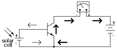
Current through the meter movement in this circuit will be β times the solar cell current. With a transistor β of 100, this represents a substantial increase in measurement sensitivity. It is prudent to point out that the additional power to move the meter needle comes from the battery on the far right of the circuit, not the solar cell itself. All the solar cell's current does is control battery current to the meter to provide a greater meter reading than the solar cell could provide unaided.
Because the transistor is a current-regulating device, and because meter movement indications are based on the amount of current through their movement coils, meter indication in this circuit should depend only on the amount of current from the solar cell, not on the amount of voltage provided by the battery. This means the accuracy of the circuit will be independent of battery condition, a significant feature! All that is required of the battery is a certain minimum voltage and current output ability to be able to drive the meter full-scale if needed.
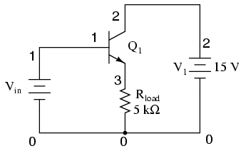
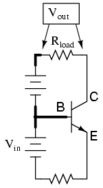
Another way in which the common-emitter configuration may be used is to produce an output voltage derived from the input signal, rather than a specific output current. Let's replace the meter movement with a plain resistor and measure voltage between collector and emitter:
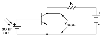
With the solar cell darkened (no current), the transistor will be in cutoff mode and behave as an open switch between collector and emitter. This will produce maximum voltage drop between collector and emitter for maximum Voutput, equal to the full voltage of the battery.
At full power (maximum light exposure), the solar cell will drive the transistor into saturation mode, making it behave like a closed switch between collector and emitter. The result will be minimum voltage drop between collector and emitter, or almost zero output voltage. In actuality, a saturated transistor can never achieve zero voltage drop between collector and emitter due to the two PN junctions through which collector current must travel. However, this "collector-emitter saturation voltage" will be fairly low, around several tenths of a volt, depending on the specific transistor used.
For light exposure levels somewhere between zero and maximum solar cell output, the transistor will be in its active mode, and the output voltage will be somewhere between zero and full battery voltage. An important quality to note here about the common-emitter configuration is that the output voltage is inversely proportional to the input signal strength. That is, the output voltage decreases as the input signal increases. For this reason, the common-emitter amplifier configuration is referred to as an inverting amplifier.
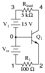
A quick SPICE simulation will verify our qualitative conclusions about this amplifier circuit:
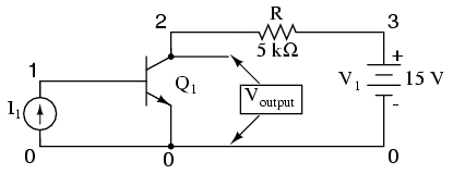
common-emitter amplifier
i1 0 1 dc
q1 2 1 0 mod1
r 3 2 5000
v1 3 0 dc 15
.model mod1 npn
.dc i1 0 50u 2u
.plot dc v(2,0)
.end
type        npn
is        1.00E-16
bf         100.000
nf           1.000
br           1.000
nr           1.000
i1         v(2)   0.000E+00    5.000E+00    1.000E+01    1.500E+01
- - - - - - - - - - - - - - - - - - - - - - - - - - - - - - - - -
0.000E+00  1.500E+01 .             .             .             *
2.000E-06  1.400E+01 .             .             .          *  .
4.000E-06  1.300E+01 .             .             .       *     .
6.000E-06  1.200E+01 .             .             .     *       .
8.000E-06  1.100E+01 .             .             .  *          .
1.000E-05  1.000E+01 .             .             *             .
1.200E-05  9.000E+00 .             .          *  .             .
1.400E-05  8.000E+00 .             .       *     .             .
1.600E-05  7.000E+00 .             .     *       .             .
1.800E-05  6.000E+00 .             .  *          .             .
2.000E-05  5.000E+00 .             *             .             .
2.200E-05  4.000E+00 .          *  .             .             .
2.400E-05  3.000E+00 .       *     .             .             .
2.600E-05  2.000E+00 .     *       .             .             .
2.800E-05  1.000E+00 .  *          .             .             .
3.000E-05  2.261E-01 .*            .             .             .
3.200E-05  1.850E-01 .*            .             .             .
3.400E-05  1.694E-01 *             .             .             .
3.600E-05  1.597E-01 *             .             .             .
3.800E-05  1.527E-01 *             .             .             .
4.000E-05  1.472E-01 *             .             .             .
4.200E-05  1.427E-01 *             .             .             .
4.400E-05  1.388E-01 *             .             .             .
4.600E-05  1.355E-01 *             .             .             .
4.800E-05  1.325E-01 *             .             .             .
5.000E-05  1.299E-01 *             .             .             .
- - - - - - - - - - - - - - - - - - - - - - - - - - - - - - - - -
At the beginning of the simulation where the current source (solar cell) is outputting zero current, the transistor is in cutoff mode and the full 15 volts from the battery is shown at the amplifier output (between nodes 2 and 0). As the solar cell's current begins to increase, the output voltage proportionally decreases, until the transistor reaches saturation at 30 µA of base current (3 mA of collector current). Notice how the output voltage trace on the graph is perfectly linear (1 volt steps from 15 volts to 1 volt) until the point of saturation, where it never quite reaches zero. This is the effect mentioned earlier, where a saturated transistor can never achieve exactly zero voltage drop between collector and emitter due to internal junction effects. What we do see is a sharp output voltage decrease from 1 volt to 0.2261 volts as the input current increases from 28 µA to 30 µA, and then a continuing decrease in output voltage from then on (albeit in progressively smaller steps). The lowest the output voltage ever gets in this simulation is 0.1299 volts, asymptotically approaching zero.
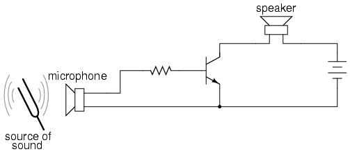
So far, we've seen the transistor used as an amplifier for DC signals. In the solar cell light meter example, we were interested in amplifying the DC output of the solar cell to drive a DC meter movement, or to produce a DC output voltage. However, this is not the only way in which a transistor may be employed as an amplifier. In many cases, what is desired is an AC amplifier for amplifying alternating current and voltage signals. One common application of this is in audio electronics (radios, televisions, and public-address systems). Earlier, we saw an example where the audio output of a tuning fork could be used to activate a transistor as a switch. Let's see if we can modify that circuit to send power to a speaker rather than to a lamp:
In the original circuit, a full-wave bridge rectifier was used to convert the microphone's AC output signal into a DC voltage to drive the input of the transistor. All we cared about here was turning the lamp on with a sound signal from the microphone, and this arrangement sufficed for that purpose. But now we want to actually reproduce the AC signal and drive a speaker. This means we cannot rectify the microphone's output anymore, because we need undistorted AC signal to drive the transistor! Let's remove the bridge rectifier and replace the lamp with a speaker:
Since the microphone may produce voltages exceeding the forward voltage drop of the base-emitter PN (diode) junction, I've placed a resistor in series with the microphone. Let's simulate this circuit now in SPICE and see what happens:
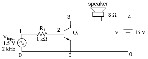
common-emitter amplifier
vinput 1 0 sin (0 1.5 2000 0 0)
r1 1 2 1k
q1 3 2 0 mod1
rspkr 3 4 8
v1 4 0 dc 15
.model mod1 npn
.tran 0.02m 0.74m
.plot tran v(1,0) i(v1)
.end
legend:
 *: v(1)
 +: i(v1)
v(1)
(*)--- -2.000E+00   -1.000E+00    0.000E+00    1.000E+00  2.000E+00
(+)--- -8.000E-02   -6.000E-02   -4.000E-02   -2.000E-02  0.000E+00
- - - - - - - - - - - - - - - - - - - - - - - - - - - - - - - - -
 0.000E+00 .             .             *             .           +
 3.725E-01 .             .             .    *        .           +
 7.195E-01 .             .             .         *   .          +.
 1.024E+00 .             .             .             *+          .
 1.264E+00 .             .             +             .   *       .
 1.420E+00 .             .   +         .             .     *     .
 1.493E+00 .            +.             .             .      *    .
 1.470E+00 .             .+            .             .      *    .
 1.351E+00 .             .        +    .             .    *      .
 1.154E+00 .             .             .       +     . *         .
 8.791E-01 .             .             .           * .        +  .
 5.498E-01 .             .             .       *     .           +
 1.877E-01 .             .             .  *          .           +
-1.872E-01 .             .          *  .             .           +
-5.501E-01 .             .     *       .             .           +
-8.815E-01 .             . *           .             .           +
-1.151E+00 .           * .             .             .           +
-1.352E+00 .        *    .             .             .           +
-1.472E+00 .      *      .             .             .           +
-1.491E+00 .      *      .             .             .           +
-1.422E+00 .       *     .             .             .           +
-1.265E+00 .         *   .             .             .           +
-1.022E+00 .             *             .             .           +
-7.205E-01 .             .   *         .             .           +
-3.723E-01 .             .        *    .             .           +
 3.040E-06 .             .             *             .           +
 3.724E-01 .             .             .    *        .           +
 7.205E-01 .             .             .         *   .          +.
 1.022E+00 .             .             .             * +         .
 1.265E+00 .             .             +             .   *       .
 1.422E+00 .             .   +         .             .     *     .
 1.491E+00 .            +.             .             .      *    .
 1.473E+00 .             .+            .             .      *    .
 1.352E+00 .             .        +    .             .    *      .
 1.151E+00 .             .             .       +     . *         .
 8.814E-01 .             .             .           * .         + .
 5.501E-01 .             .             .       *     .           +
 1.880E-01 .             .             .  *          .           +
- - - - - - - - - - - - - - - - - - - - - - - - - - - - - - - - -
The simulation plots both the input voltage (an AC signal of 1.5 volt peak amplitude and 2000 Hz frequency) and the current through the 15 volt battery, which is the same as the current through the speaker. What we see here is a full AC sine wave alternating in both positive and negative directions, and a half-wave output current waveform that only pulses in one direction. If we were actually driving a speaker with this waveform, the sound produced would be horribly distorted.
What's wrong with the circuit? Why won't it faithfully reproduce the entire AC waveform from the microphone? The answer to this question is found by close inspection of the transistor diode-regulating diode model:
Collector current is controlled, or regulated, through the constant-current mechanism according to the pace set by the current through the base-emitter diode. Note that both current paths through the transistor are monodirectional: one way only! Despite our intent to use the transistor to amplify an AC signal, it is essentially a DC device, capable of handling currents in a single direction only. We may apply an AC voltage input signal between the base and emitter, but electrons cannot flow in that circuit during the part of the cycle that reverse-biases the base-emitter diode junction. Therefore, the transistor will remain in cutoff mode throughout that portion of the cycle. It will "turn on" in its active mode only when the input voltage is of the correct polarity to forward-bias the base-emitter diode, and only when that voltage is sufficiently high to overcome the diode's forward voltage drop. Remember that bipolar transistors are current-controlled devices: they regulate collector current based on the existence of base-to-emitter current, not base-to-emitter voltage.
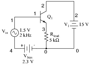
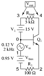
The only way we can get the transistor to reproduce the entire waveform as current through the speaker is to keep the transistor in its active mode the entire time. This means we must maintain current through the base during the entire input waveform cycle. Consequently, the base-emitter diode junction must be kept forward-biased at all times. Fortunately, this can be accomplished with the aid of a DC bias voltage added to the input signal. By connecting a sufficient DC voltage in series with the AC signal source, forward-bias can be maintained at all points throughout the wave cycle:
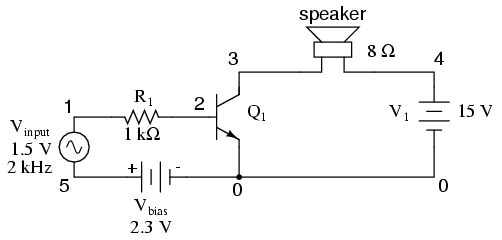
common-emitter amplifier
vinput 1 5 sin (0 1.5 2000 0 0)
vbias 5 0 dc 2.3
r1 1 2 1k
q1 3 2 0 mod1
rspkr 3 4 8
v1 4 0 dc 15
.model mod1 npn
.tran 0.02m 0.78m
.plot tran v(1,0) i(v1)
.end
legend:
*: v(1)
+: i(v1)
v(1)
(*)---  0.000E+00   1.000E+00    2.000E+00    3.000E+00  4.000E+00
(+)--- -3.000E-01  -2.000E-01   -1.000E-01    0.000E+00  1.000E-01
- - - - - - - - - - - - - - - - - - - - - - - - - - - - - - - - -
2.300E+00 .             .       +     .   *         .           .
2.673E+00 .             .  +          .        *    .           .
3.020E+00 .            +.             .             *           .
3.322E+00 .       +     .             .             .    *      .
3.563E+00 .    +        .             .             .       *   .
3.723E+00 .  +          .             .             .         * .
3.790E+00 . +           .             .             .          *.
3.767E+00 . +           .             .             .          *.
3.657E+00 .   +         .             .             .        *  .
3.452E+00 .      +      .             .             .     *     .
3.177E+00 .         +   .             .             . *         .
2.850E+00 .             .+            .           * .           .
2.488E+00 .             .     +       .      *      .           .
2.113E+00 .             .          +  . *           .           .
1.750E+00 .             .          *  . +           .           .
1.419E+00 .             .     *       .     +       .           .
1.148E+00 .             . *           .         +   .           .
9.493E-01 .            *.             .           + .           .
8.311E-01 .           * .             .             +           .
8.050E-01 .          *  .             .             +           .
8.797E-01 .           * .             .            +.           .
1.039E+00 .             .*            .          +  .           .
1.275E+00 .             .   *         .       +     .           .
1.579E+00 .             .       *     .   +         .           .
1.929E+00 .             .            *+             .           .
2.300E+00 .             .       +     .   *         .           .
2.673E+00 .             .  +          .        *    .           .
3.019E+00 .            +.             .             *           .
3.322E+00 .       +     .             .             .    *      .
3.564E+00 .    +        .             .             .       *   .
3.722E+00 .  +          .             .             .         * .
3.790E+00 . +           .             .             .          *.
3.768E+00 . +           .             .             .          *.
3.657E+00 .   +         .             .             .        *  .
3.451E+00 .      +      .             .             .     *     .
3.178E+00 .         +   .             .             . *         .
2.851E+00 .             .+            .           * .           .
2.488E+00 .             .     +       .      *      .           .
2.113E+00 .             .          +  . *           .           .
1.748E+00 .             .         *   . +           .           .
- - - - - - - - - - - - - - - - - - - - - - - - - - - - - - - - -
With the bias voltage source of 2.3 volts in place, the transistor remains in its active mode throughout the entire cycle of the wave, faithfully reproducing the waveform at the speaker. Notice that the input voltage (measured between nodes 1 and 0) fluctuates between about 0.8 volts and 3.8 volts, a peak-to-peak voltage of 3 volts just as expected (source voltage = 1.5 volts peak). The output (speaker) current varies between zero and almost 300 mA, 180o out of phase with the input (microphone) signal.
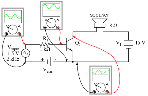
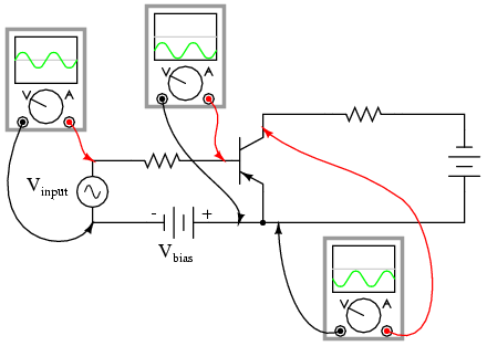
The following illustration is another view of the same circuit, this time with a few oscilloscopes ("scopemeters") connected at crucial points to display all the pertinent signals:
The need for biasing a transistor amplifier circuit to obtain full waveform reproduction is an important consideration. A separate section of this chapter will be devoted entirely to the subject biasing and biasing techniques. For now, it is enough to understand that biasing may be necessary for proper voltage and current output from the amplifier.
Now that we have a functioning amplifier circuit, we can investigate its voltage, current, and power gains. The generic transistor used in these SPICE analyses has a β of 100, as indicated by the short transistor statistics printout included in the text output (these statistics were cut from the last two analyses for brevity's sake):
type        npn
is        1.00E-16
bf         100.000
nf           1.000
br           1.000
nr           1.000
β is listed under the abbreviation "bf," which actually stands for "beta, forward". If we wanted to insert our own β ratio for an analysis, we could have done so on the .model line of the SPICE netlist.
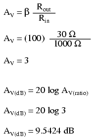
Since β is the ratio of collector current to base current, and we have our load connected in series with the collector terminal of the transistor and our source connected in series with the base, the ratio of output current to input current is equal to beta. Thus, our current gain for this example amplifier is 100, or 40 dB.
Voltage gain is a little more complicated to figure than current gain for this circuit. As always, voltage gain is defined as the ratio of output voltage divided by input voltage. In order to experimentally determine this, we need to modify our last SPICE analysis to plot output voltage rather than output current so we have two voltage plots to compare:
common-emitter amplifier
vinput 1 5 sin (0 1.5 2000 0 0)
vbias 5 0 dc 2.3
r1 1 2 1k
q1 3 2 0 mod1
rspkr 3 4 8
v1 4 0 dc 15
.model mod1 npn
.tran 0.02m 0.78m
.plot tran v(1,0) v(4,3)
.end
legend:
*: v(1)
+: v(4,3)
v(1)
(*+)-  0.000E+00    1.000E+00    2.000E+00    3.000E+00  4.000E+00
- - - - - - - - - - - - - - - - - - - - - - - - - - - - - - - - -
2.300E+00 .             . +           .   *         .            .
2.673E+00 .             .     +       .        *    .            .
3.020E+00 .             .         +   .             *            .
3.322E+00 .             .            +.             .    *       .
3.563E+00 .             .             . +           .       *    .
3.723E+00 .             .             .  +          .         *  .
3.790E+00 .             .             .   +         .          * .
3.767E+00 .             .             .   +         .          * .
3.657E+00 .             .             .  +          .        *   .
3.452E+00 .             .             +             .     *      .
3.177E+00 .             .          +  .             . *          .
2.850E+00 .             .       +     .           * .            .
2.488E+00 .             .   +         .      *      .            .
2.113E+00 .             +             . *           .            .
1.750E+00 .         +   .          *  .             .            .
1.419E+00 .     +       .     *       .             .            .
1.148E+00 .  +          . *           .             .            .
9.493E-01 .+           *.             .             .            .
8.311E-01 +           * .             .             .            .
8.050E-01 +          *  .             .             .            .
8.797E-01 .+          * .             .             .            .
1.039E+00 . +           .*            .             .            .
1.275E+00 .    +        .   *         .             .            .
1.579E+00 .       +     .       *     .             .            .
1.929E+00 .           + .            *.             .            .
2.300E+00 .             . +           .   *         .            .
2.673E+00 .             .     +       .        *    .            .
3.019E+00 .             .         +   .             *            .
3.322E+00 .             .            +.             .    *       .
3.564E+00 .             .             . +           .       *    .
3.722E+00 .             .             .  +          .         *  .
3.790E+00 .             .             .   +         .          * .
3.768E+00 .             .             .   +         .          * .
3.657E+00 .             .             .  +          .        *   .
3.451E+00 .             .             +             .     *      .
3.178E+00 .             .          +  .             . *          .
2.851E+00 .             .       +     .           * .            .
2.488E+00 .             .   +         .      *      .            .
2.113E+00 .             +             . *           .            .
1.748E+00 .         +   .         *   .             .            .
- - - - - - - - - - - - - - - - - - - - - - - - - - - - - - - - -
Plotted on the same scale (from 0 to 4 volts), we see that the output waveform ("+") has a smaller peak-to-peak amplitude than the input waveform ("*"), in addition to being at a lower bias voltage, not elevated up from 0 volts like the input. Since voltage gain for an AC amplifier is defined by the ratio of AC amplitudes, we can ignore any DC bias separating the two waveforms. Even so, the input waveform is still larger than the output, which tells us that the voltage gain is less than 1 (a negative dB figure).
To be honest, this low voltage gain is not characteristic to all common-emitter amplifiers. In this case it is a consequence of the great disparity between the input and load resistances. Our input resistance (R1) here is 1000 Ω, while the load (speaker) is only 8 Ω. Because the current gain of this amplifier is determined solely by the β of the transistor, and because that β figure is fixed, the current gain for this amplifier won't change with variations in either of these resistances. However, voltage gain is dependent on these resistances. If we alter the load resistance, making it a larger value, it will drop a proportionately greater voltage for its range of load currents, resulting in a larger output waveform. Let's try another simulation, only this time with a 30 Ω load instead of an 8 Ω load:
common-emitter amplifier
vinput 1 5 sin (0 1.5 2000 0 0)
vbias 5 0 dc 2.3
r1 1 2 1k
q1 3 2 0 mod1
rspkr 3 4 30
v1 4 0 dc 15
.model mod1 npn
.tran 0.02m 0.78m
.plot tran v(1,0) v(4,3)
.end
legend:
 *: v(1)
 +: v(4,3)
v(1)
(*)--  0.000E+00    1.000E+00    2.000E+00    3.000E+00  4.000E+00
(+)-- -5.000E+00    0.000E+00    5.000E+00    1.000E+01  1.500E+01
- - - - - - - - - - - - - - - - - - - - - - - - - - - - - - - - -
2.300E+00 .             .           + .   *         .            .
2.673E+00 .             .             .+       *    .            .
3.020E+00 .             .             .   +         *            .
3.322E+00 .             .             .     +       .    *       .
3.563E+00 .             .             .       +     .       *    .
3.723E+00 .             .             .         +   .         *  .
3.790E+00 .             .             .         +   .          * .
3.767E+00 .             .             .         +   .          * .
3.657E+00 .             .             .        +    .        *   .
3.452E+00 .             .             .      +      .     *      .
3.177E+00 .             .             .    +        . *          .
2.850E+00 .             .             . +         * .            .
2.488E+00 .             .            +.      *      .            .
2.113E+00 .             .         +   . *           .            .
1.750E+00 .             .      +   *  .             .            .
1.419E+00 .             .    +*       .             .            .
1.148E+00 .             . x           .             .            .
9.493E-01 .            *.+            .             .            .
8.311E-01 .           * +             .             .            .
8.050E-01 .          *  +             .             .            .
8.797E-01 .           * .+            .             .            .
1.039E+00 .             .*+           .             .            .
1.275E+00 .             .  +*         .             .            .
1.579E+00 .             .     + *     .             .            .
1.929E+00 .             .        +   *.             .            .
2.300E+00 .             .           + .   *         .            .
2.673E+00 .             .             .+       *    .            .
3.019E+00 .             .             .   +         *            .
3.322E+00 .             .             .     +       .    *       .
3.564E+00 .             .             .       +     .       *    .
3.722E+00 .             .             .         +   .         *  .
3.790E+00 .             .             .         +   .          * .
3.768E+00 .             .             .         +   .          * .
3.657E+00 .             .             .        +    .        *   .
3.451E+00 .             .             .      +      .     *      .
3.178E+00 .             .             .    +        . *          .
2.851E+00 .             .             . +         * .            .
2.488E+00 .             .            +.      *      .            .
2.113E+00 .             .         +   . *           .            .
1.748E+00 .             .      +  *   .             .            .
- - - - - - - - - - - - - - - - - - - - - - - - - - - - - - - - -
This time the output voltage waveform is significantly greater in amplitude than the input waveform. This may not be obvious at first, since the two waveforms are plotted on different scales: the input on a scale of 0 to 4 volts and the output on a scale of -5 to 15 volts. Looking closely, we can see that the output waveform ("+") crests between 0 and about 9 volts: approximately 3 times the amplitude of the input voltage.
We can perform another computer analysis of this circuit, only this time instructing SPICE to analyze it from an AC point of view, giving us peak voltage figures for input and output instead of a time-based plot of the waveforms:
common-emitter amplifier
vinput 1 5 ac 1.5
vbias 5 0 dc 2.3
r1 1 2 1k
q1 3 2 0 mod1
rspkr 3 4 30
v1 4 0 dc 15
.model mod1 npn
.ac lin 1 2000 2000
.print ac v(1,0) v(4,3)
.end
freq          v(1)        v(4,3)
2.000E+03     1.500E+00   4.418E+00
Peak voltage measurements of input and output show an input of 1.5 volts and an output of 4.418 volts. This gives us a voltage gain ratio of 2.9453 (4.418 V / 1.5 V), or 9.3827 dB.

Because the current gain of the common-emitter amplifier is fixed by β, and since the input and output voltages will be equal to the input and output currents multiplied by their respective resistors, we can derive an equation for approximate voltage gain:
As you can see, the predicted results for voltage gain are quite close to the simulated results. With perfectly linear transistor behavior, the two sets of figures would exactly match. SPICE does a reasonable job of accounting for the many "quirks" of bipolar transistor function in its analysis, hence the slight mismatch in voltage gain based on SPICE's output.
These voltage gains remain the same regardless of where we measure output voltage in the circuit: across collector and emitter, or across the series load resistor as we did in the last analysis. The amount of output voltage change for any given amount of input voltage will remain the same. Consider the two following SPICE analyses as proof of this. The first simulation is time-based, to provide a plot of input and output voltages. You will notice that the two signals are 180o out of phase with each other. The second simulation is an AC analysis, to provide simple, peak voltage readings for input and output:
common-emitter amplifier
vinput 1 5 sin (0 1.5 2000 0 0)
vbias 5 0 dc 2.3
r1 1 2 1k
q1 3 2 0 mod1
rspkr 3 4 30
v1 4 0 dc 15
.model mod1 npn
.tran 0.02m 0.74m
.plot tran v(1,0) v(3,0)
.end
legend:
*: v(1)
+: v(3)
v(1)
(*)--  0.000E+00     1.000E+00     2.000E+00     3.000E+00  4.000E+00
(+)--  0.000E+00     5.000E+00     1.000E+01     1.500E+01  2.000E+01
- - - - - - - - - - - - - - - - - - - - - - - - - - - - - - - - -
 2.300E+00 .           .             . + *         .             .
 2.673E+00 .           .            +.        *    .             .
 3.020E+00 .           .         +   .             *             .
 3.324E+00 .           .       +     .             .    *        .
 3.564E+00 .           .     +       .             .       *     .
 3.720E+00 .           .   +         .             .         *   .
 3.793E+00 .           .   +         .             .          *  .
 3.770E+00 .           .   +         .             .          *  .
 3.651E+00 .           .    +        .             .        *    .
 3.454E+00 .           .      +      .             .     *       .
 3.179E+00 .           .        +    .             .  *          .
 2.850E+00 .           .           + .           * .             .
 2.488E+00 .           .             .+     *      .             .
 2.113E+00 .           .             . * +         .             .
 1.750E+00 .           .         *   .      +      .             .
 1.418E+00 .           .     *       .        +    .             .
 1.149E+00 .           . *           .           + .             .
 9.477E-01 .          *.             .            +.             .
 8.277E-01 .         * .             .             +             .
 8.091E-01 .        *  .             .             +             .
 8.781E-01 .         * .             .            +.             .
 1.035E+00 .           *             .           + .             .
 1.278E+00 .           .   *         .          +  .             .
 1.579E+00 .           .       *     .       +     .             .
 1.928E+00 .           .            *.    +        .             .
 2.300E+00 .           .             . + *         .             .
 2.672E+00 .           .            +.        *    .             .
 3.020E+00 .           .         +   .             *             .
 3.322E+00 .           .       +     .             .    *        .
 3.565E+00 .           .     +       .             .       *     .
 3.722E+00 .           .   +         .             .         *   .
 3.791E+00 .           .   +         .             .          *  .
 3.773E+00 .           .   +         .             .          *  .
 3.652E+00 .           .    +        .             .        *    .
 3.451E+00 .           .      +      .             .     *       .
 3.181E+00 .           .        +    .             .  *          .
 2.850E+00 .           .           + .           * .             .
 2.488E+00 .           .             .+     *      .             .
- - - - - - - - - - - - - - - - - - - - - - - - - - - - - - - - -
common-emitter amplifier
vinput 1 5 ac 1.5
vbias 5 0 dc 2.3
r1 1 2 1k
q1 3 2 0 mod1
rspkr 3 4 30
v1 4 0 dc 15
.model mod1 npn
.ac lin 1 2000 2000
.print ac v(1,0) v(3,0)
.end
freq          v(1)        v(3)
2.000E+03     1.500E+00   4.418E+00
We still have a peak output voltage of 4.418 volts with a peak input voltage of 1.5 volts. The only difference from the last set of simulations is the phase of the output voltage.
So far, the example circuits shown in this section have all used NPN transistors. PNP transistors are just as valid to use as NPN in any amplifier configuration, so long as the proper polarity and current directions are maintained, and the common-emitter amplifier is no exception. The inverting behavior and gain properties of a PNP transistor amplifier are the same as its NPN counterpart, just the polarities are different:
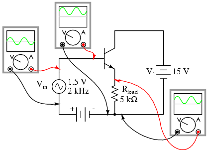
Our next transistor configuration to study is a bit simpler in terms of gain calculations. Called the common-collector configuration, its schematic diagram looks like this:
It is called the common-collector configuration because (ignoring the power supply battery) both the signal source and the load share the collector lead as a common connection point:
It should be apparent that the load resistor in the common-collector amplifier circuit receives both the base and collector currents, being placed in series with the emitter. Since the emitter lead of a transistor is the one handling the most current (the sum of base and collector currents, since base and collector currents always mesh together to form the emitter current), it would be reasonable to presume that this amplifier will have a very large current gain (maximum output current for minimum input current). This presumption is indeed correct: the current gain for a common-collector amplifier is quite large, larger than any other transistor amplifier configuration. However, this is not necessarily what sets it apart from other amplifier designs.
Let's proceed immediately to a SPICE analysis of this amplifier circuit, and you will be able to immediately see what is unique about this amplifier:
common-collector amplifier
vin 1 0
q1 2 1 3 mod1
v1 2 0 dc 15
rload 3 0 5k
.model mod1 npn
.dc vin 0 5 0.2
.plot dc v(3,0)
.end
type        npn
is        1.00E-16
bf         100.000
nf           1.000
br           1.000
nr           1.000
vin        v(3)  0.000E+00     2.000E+00    4.000E+00    6.000E+00
- - - - - - - - - - - - - - - - - - - - - - - - - - - - - - - - -
0.000E+00  7.500E-08 *             .             .             .
2.000E-01  7.501E-08 *             .             .             .
4.000E-01  2.704E-06 *             .             .             .
6.000E-01  4.954E-03 *             .             .             .
8.000E-01  1.221E-01 .*            .             .             .
1.000E+00  2.989E-01 . *           .             .             .
1.200E+00  4.863E-01 .  *          .             .             .
1.400E+00  6.777E-01 .    *        .             .             .
1.600E+00  8.712E-01 .     *       .             .             .
1.800E+00  1.066E+00 .      *      .             .             .
2.000E+00  1.262E+00 .        *    .             .             .
2.200E+00  1.458E+00 .         *   .             .             .
2.400E+00  1.655E+00 .           * .             .             .
2.600E+00  1.852E+00 .            *.             .             .
2.800E+00  2.049E+00 .             *             .             .
3.000E+00  2.247E+00 .             . *           .             .
3.200E+00  2.445E+00 .             .  *          .             .
3.400E+00  2.643E+00 .             .   *         .             .
3.600E+00  2.841E+00 .             .     *       .             .
3.800E+00  3.039E+00 .             .      *      .             .
4.000E+00  3.237E+00 .             .        *    .             .
4.200E+00  3.436E+00 .             .         *   .             .
4.400E+00  3.634E+00 .             .          *  .             .
4.600E+00  3.833E+00 .             .            *.             .
4.800E+00  4.032E+00 .             .             *             .
5.000E+00  4.230E+00 .             .             . *           .
- - - - - - - - - - - - - - - - - - - - - - - - - - - - - - - - -
Unlike the common-emitter amplifier from the previous section, the common-collector produces an output voltage in direct rather than inverse proportion to the rising input voltage. As the input voltage increases, so does the output voltage. More than that, a close examination reveals that the output voltage is nearly identical to the input voltage, lagging behind only about 0.77 volts.
This is the unique quality of the common-collector amplifier: an output voltage that is nearly equal to the input voltage. Examined from the perspective of output voltage change for a given amount of input voltage change, this amplifier has a voltage gain of almost exactly unity (1), or 0 dB. This holds true for transistors of any β value, and for load resistors of any resistance value.
It is simple to understand why the output voltage of a common-collector amplifier is always nearly equal to the input voltage. Referring back to the diode-regulating diode transistor model, we see that the base current must go through the base-emitter PN junction, which is equivalent to a normal rectifying diode. So long as this junction is forward-biased (the transistor conducting current in either its active or saturated modes), it will have a voltage drop of approximately 0.7 volts, assuming silicon construction. This 0.7 volt drop is largely irrespective of the actual magnitude of base current, so we can regard it as being constant:
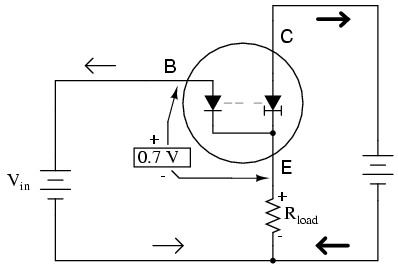
Given the voltage polarities across the base-emitter PN junction and the load resistor, we see that they must add together to equal the input voltage, in accordance with Kirchhoff's Voltage Law. In other words, the load voltage will always be about 0.7 volts less than the input voltage for all conditions where the transistor is conducting. Cutoff occurs at input voltages below 0.7 volts, and saturation at input voltages in excess of battery (supply) voltage plus 0.7 volts.
Because of this behavior, the common-collector amplifier circuit is also known as the voltage-follower or emitter-follower amplifier, in reference to the fact that the input and load voltages follow each other so closely.
Applying the common-collector circuit to the amplification of AC signals requires the same input "biasing" used in the common-emitter circuit: a DC voltage must be added to the AC input signal to keep the transistor in its active mode during the entire cycle. When this is done, the result is a non-inverting amplifier:
common-collector amplifier
vin 1 4 sin(0 1.5 2000 0 0)
vbias 4 0 dc 2.3
q1 2 1 3 mod1
v1 2 0 dc 15
rload 3 0 5k
.model mod1 npn
.tran .02m .78m
.plot tran v(1,0) v(3,0)
.end
legend:
*: v(1)
+: v(3)
v(1)   0.000E+00   1.000E+00     2.000E+00    3.000E+00  4.000E+00
- - - - - - - - - - - - - - - - - - - - - - - - - - - - - - - - -
2.300E+00 .            .       +     .   *         .            .
2.673E+00 .            .            +.        *    .            .
3.020E+00 .            .             .   +         *            .
3.322E+00 .            .             .       +     .    *       .
3.563E+00 .            .             .          +  .       *    .
3.723E+00 .            .             .            +.         *  .
3.790E+00 .            .             .             +          * .
3.767E+00 .            .             .             +          * .
3.657E+00 .            .             .            +.        *   .
3.452E+00 .            .             .         +   .     *      .
3.177E+00 .            .             .     +       . *          .
2.850E+00 .            .             .+          * .            .
2.488E+00 .            .         +   .      *      .            .
2.113E+00 .            .    +        . *           .            .
1.750E+00 .            +          *  .             .            .
1.419E+00 .        +   .     *       .             .            .
1.148E+00 .    +       . *           .             .            .
9.493E-01 .  +        *.             .             .            .
8.311E-01 .+         * .             .             .            .
8.050E-01 .+        *  .             .             .            .
8.797E-01 . +        * .             .             .            .
1.039E+00 .   +        .*            .             .            .
1.275E+00 .      +     .   *         .             .            .
1.579E+00 .          + .       *     .             .            .
1.929E+00 .            .  +         *.             .            .
2.300E+00 .            .       +     .   *         .            .
2.673E+00 .            .            +.        *    .            .
3.019E+00 .            .             .   +         *            .
3.322E+00 .            .             .       +     .    *       .
3.564E+00 .            .             .          +  .       *    .
3.722E+00 .            .             .            +.         *  .
3.790E+00 .            .             .             +          * .
3.768E+00 .            .             .             +          * .
3.657E+00 .            .             .            +.        *   .
3.451E+00 .            .             .         +   .     *      .
3.178E+00 .            .             .     +       . *          .
2.851E+00 .            .             .+          * .            .
2.488E+00 .            .         +   .      *      .            .
2.113E+00 .            .    +        . *           .            .
1.748E+00 .            +         *   .             .            .
- - - - - - - - - - - - - - - - - - - - - - - - - - - - - - - - -
Here's another view of the circuit, this time with oscilloscopes connected to several points of interest:
Since this amplifier configuration doesn't provide any voltage gain (in fact, in practice it actually has a voltage gain of slightly less than 1), its only amplifying factor is current. The common-emitter amplifier configuration examined in the previous section had a current gain equal to the β of the transistor, being that the input current went through the base and the output (load) current went through the collector, and β by definition is the ratio between the collector and emitter currents. In the common-collector configuration, though, the load is situated in series with the emitter, and thus its current is equal to the emitter current. With the emitter carrying collector current and base current, the load in this type of amplifier has all the current of the collector running through it plus the input current of the base. This yields a current gain of β plus 1:
Once again, PNP transistors are just as valid to use in the common-collector configuration as NPN transistors. The gain calculations are all the same, as is the non-inverting behavior of the amplifier. The only difference is in voltage polarities and current directions:
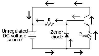
A popular application of the common-collector amplifier is for regulated DC power supplies, where an unregulated (varying) source of DC voltage is clipped at a specified level to supply regulated (steady) voltage to a load. Of course, zener diodes already provide this function of voltage regulation:
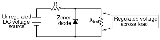
However, when used in this direct fashion, the amount of current that may be supplied to the load is usually quite limited. In essence, this circuit regulates voltage across the load by keeping current through the series resistor at a high enough level to drop all the excess power source voltage across it, the zener diode drawing more or less current as necessary to keep the voltage across itself steady. For high-current loads, an plain zener diode voltage regulator would have to be capable of shunting a lot of current through the diode in order to be effective at regulating load voltage in the event of large load resistance or voltage source changes.
One popular way to increase the current-handling ability of a regulator circuit like this is to use a common-collector transistor to amplify current to the load, so that the zener diode circuit only has to handle the amount of current necessary to drive the base of the transistor:
There's really only one caveat to this approach: the load voltage will be approximately 0.7 volts less than the zener diode voltage, due to the transistor's 0.7 volt base-emitter drop. However, since this 0.7 volt difference is fairly constant over a wide range of load currents, a zener diode with a 0.7 volt higher rating can be chosen for the application.
Sometimes the high current gain of a single-transistor, common-collector configuration isn't enough for a particular application. If this is the case, multiple transistors may be staged together in a popular configuration known as a Darlington pair, just an extension of the common-collector concept:
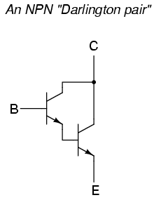
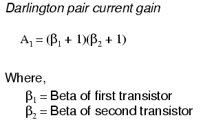
Darlington pairs essentially place one transistor as the common-collector load for another transistor, thus multiplying their individual current gains. Base current through the upper-left transistor is amplified through that transistor's emitter, which is directly connected to the base of the lower-right transistor, where the current is again amplified. The overall current gain is as follows:
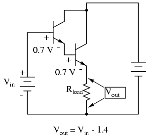
Voltage gain is still nearly equal to 1 if the entire assembly is connected to a load in common-collector fashion, although the load voltage will be a full 1.4 volts less than the input voltage:
Darlington pairs may be purchased as discrete units (two transistors in the same package), or may be built up from a pair of individual transistors. Of course, if even more current gain is desired than what may be obtained with a pair, Darlington triplet or quadruplet assemblies may be constructed.
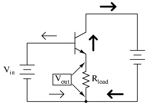
The final transistor amplifier configuration we need to study is the common-base. This configuration is more complex than the other two, and is less common due to its strange operating characteristics.
It is called the common-base configuration because (DC power source aside), the signal source and the load share the base of the transistor as a common connection point:
Perhaps the most striking characteristic of this configuration is that the input signal source must carry the full emitter current of the transistor, as indicated by the heavy arrows in the first illustration. As we know, the emitter current is greater than any other current in the transistor, being the sum of base and collector currents. In the last two amplifier configurations, the signal source was connected to the base lead of the transistor, thus handling the least current possible.
Because the input current exceeds all other currents in the circuit, including the output current, the current gain of this amplifier is actually less than 1 (notice how Rload is connected to the collector, thus carrying slightly less current than the signal source). In other words, it attenuates current rather than amplifying it. With common-emitter and common-collector amplifier configurations, the transistor parameter most closely associated with gain was β. In the common-base circuit, we follow another basic transistor parameter: the ratio between collector current and emitter current, which is a fraction always less than 1. This fractional value for any transistor is called the alpha ratio, or α ratio.
Since it obviously can't boost signal current, it only seems reasonable to expect it to boost signal voltage. A SPICE simulation will vindicate that assumption:
common-base amplifier
vin 0 1
r1 1 2 100
q1 4 0 2 mod1
v1 3 0 dc 15
rload 3 4 5k
.model mod1 npn
.dc vin 0.6 1.2 .02
.plot dc v(3,4)
.end
v(3,4)  0.000E+00   5.000E+00     1.000E+01    1.500E+01  2.000E+01
- - - - - - - - - - - - - - - - - - - - - - - - - - - - - - - - -
5.913E-03 *             .             .             .            .
1.274E-02 *             .             .             .            .
2.730E-02 *             .             .             .            .
5.776E-02 *             .             .             .            .
1.193E-01 *             .             .             .            .
2.358E-01 .*            .             .             .            .
4.370E-01 .*            .             .             .            .
7.447E-01 . *           .             .             .            .
1.163E+00 .  *          .             .             .            .
1.682E+00 .    *        .             .             .            .
2.281E+00 .     *       .             .             .            .
2.945E+00 .       *     .             .             .            .
3.657E+00 .         *   .             .             .            .
4.408E+00 .           * .             .             .            .
5.189E+00 .             .*            .             .            .
5.995E+00 .             .  *          .             .            .
6.820E+00 .             .    *        .             .            .
7.661E+00 .             .      *      .             .            .
8.516E+00 .             .         *   .             .            .
9.382E+00 .             .           * .             .            .
1.026E+01 .             .             .*            .            .
1.114E+01 .             .             .  *          .            .
1.203E+01 .             .             .     *       .            .
1.293E+01 .             .             .       *     .            .
1.384E+01 .             .             .          *  .            .
1.474E+01 .             .             .            *.            .
1.563E+01 .             .             .             . *          .
1.573E+01 .             .             .             . *          .
1.575E+01 .             .             .             . *          .
1.576E+01 .             .             .             . *          .
1.576E+01 .             .             .             . *          .
- - - - - - - - - - - - - - - - - - - - - - - - - - - - - - - - -
Notice how in this simulation the output voltage goes from practically nothing (cutoff) to 15.75 volts (saturation) with the input voltage being swept over a range of 0.6 volts to 1.2 volts. In fact, the output voltage plot doesn't show a rise until about 0.7 volts at the input, and cuts off (flattens) at about 1.12 volts input. This represents a rather large voltage gain with an output voltage span of 15.75 volts and an input voltage span of only 0.42 volts: a gain ratio of 37.5, or 31.48 dB. Notice also how the output voltage (measured across Rload) actually exceeds the power supply (15 volts) at saturation, due to the series-aiding effect of the the input voltage source.
A second set of SPICE analyses with an AC signal source (and DC bias voltage) tells the same story: a high voltage gain.
common-base amplifier
vin 0 1 sin (0 0.12 2000 0 0)
vbias 1 5 dc 0.95
r1 5 2 100
q1 4 0 2 mod1
v1 3 0 dc 15
rload 3 4 5k
.model mod1 npn
.tran 0.02m 0.78m
.plot tran v(1,0) v(4,3)
.end
legend:

 *: v(1)
 +: v(4,3)

v(1)
(*)-- -2.000E-01    -1.000E-01     0.000E+00     1.000E-01  2.000E-01
(+)-- -1.500E+01    -1.000E+01    -5.000E+00     0.000E+00  5.000E+00
- - - - - - - - - - - - - - - - - - - - - - - - - - - - - - - - -
0.000E+00  .             .    +        *             .           .
-2.984E-02 .             . +       *   .             .           .
-5.757E-02 .           + .     *       .             .           .
-8.176E-02 .        +    .  *          .             .           .
-1.011E-01 .      +      *             .             .           .
-1.139E-01 .    +      * .             .             .           .
-1.192E-01 .    +     *  .             .             .           .
-1.174E-01 .    +      * .             .             .           .
-1.085E-01 .     +      *.             .             .           .
-9.213E-02 .       +     .*            .             .           .
-7.020E-02 .          +  .   *         .             .           .
-4.404E-02 .             +       *     .             .           .
-1.502E-02 .             .   +       * .             .           .
1.496E-02  .             .      +      . *           .           .
4.400E-02  .             .          +  .     *       .           .
7.048E-02  .             .             +         *   .           .
9.214E-02  .             .             . +          *.           .
1.081E-01  .             .             .   +         .*          .
1.175E-01  .             .             .    +        . *         .
1.196E-01  .             .             .    +        .  *        .
1.136E-01  .             .             .   +         . *         .
1.009E-01  .             .             .  +          *           .
8.203E-02  .             .             .+         *  .           .
5.764E-02  .             .           + .       *     .           .
2.970E-02  .             .        +    .   *         .           .
-1.440E-05 .             .    +        *             .           .
-2.981E-02 .             . +       *   .             .           .
-5.755E-02 .           + .     *       .             .           .
-8.178E-02 .        +    .  *          .             .           .
-1.011E-01 .      +      *             .             .           .
-1.138E-01 .    +      * .             .             .           .
-1.192E-01 .    +     *  .             .             .           .
-1.174E-01 .    +      * .             .             .           .
-1.085E-01 .     +      *.             .             .           .
-9.209E-02 .       +     .*            .             .           .
-7.020E-02 .          +  .   *         .             .           .
-4.407E-02 .             +       *     .             .           .
-1.502E-02 .             .   +       * .             .           .
1.496E-02  .             .      +      . *           .           .
4.417E-02  .             .          +  .     *       .           .
- - - - - - - - - - - - - - - - - - - - - - - - - - - - - - - - -
As you can see, the input and output waveforms are in phase with each other. This tells us that the common-base amplifier is non-inverting.
common-base amplifier
vin 0 1 ac 0.12
vbias 1 5 dc 0.95
r1 5 2 100
q1 4 0 2 mod1
v1 3 0 dc 15
rload 3 4 5k
.model mod1 npn
.ac lin 1 2000 2000
.print ac v(1,0) v(3,4)
.end
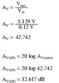
freq          v(1)        v(3,4)
2.000E+03     1.200E-01   5.129E+00
Voltage figures from the second analysis (AC mode) show a voltage gain of 42.742 (5.129 V / 0.12 V), or 32.617 dB:
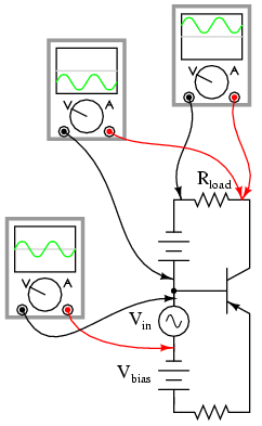
Here's another view of the circuit, showing the phase relations and DC offsets of various signals in the circuit just simulated:

. . . and for a PNP transistor:
Predicting voltage gain for the common-base amplifier configuration is quite difficult, and involves approximations of transistor behavior that are difficult to measure directly. Unlike the other amplifier configurations, where voltage gain was either set by the ratio of two resistors (common-emitter), or fixed at an unchangeable value (common-collector), the voltage gain of the common-base amplifier depends largely on the amount of DC bias on the input signal. As it turns out, the internal transistor resistance between emitter and base plays a major role in determining voltage gain, and this resistance changes with different levels of current through the emitter.
While this phenomenon is difficult to explain, it is rather easy to demonstrate through the use of computer simulation. What I'm going to do here is run several SPICE simulations on a common-base amplifier circuit, changing the DC bias voltage slightly while keeping the AC signal amplitude and all other circuit parameters constant. As the voltage gain changes from one simulation to another, different output voltage amplitudes will be noticed as a result.
Although these analyses will all be conducted in the AC mode, they were first "proofed" in the transient analysis mode (voltage plotted over time) to ensure that the entire wave was being faithfully reproduced and not "clipped" due to improper biasing. No meaningful calculations of gain can be based on waveforms that are distorted:
common-base amplifier DC bias = 0.85 volts
vin 0 1 ac 0.08
vbias 1 5 dc 0.85
r1 5 2 100
q1 4 0 2 mod1
v1 3 0 dc 15
rload 3 4 5k
.model mod1 npn
.ac lin 1 2000 2000
.print ac v(1,0) v(3,4)
.end
freq          v(1)        v(3,4)
2.000E+03     8.000E-02   3.005E+00
common-base amplifier dc bias = 0.9 volts
vin 0 1 ac 0.08
vbias 1 5 dc 0.90
r1 5 2 100
q1 4 0 2 mod1
v1 3 0 dc 15
rload 3 4 5k
.model mod1 npn
.ac lin 1 2000 2000
.print ac v(1,0) v(3,4)
.end
freq          v(1)        v(3,4)
2.000E+03     8.000E-02   3.264E+00
common-base amplifier dc bias = 0.95 volts
vin 0 1 ac 0.08
vbias 1 5 dc 0.95
r1 5 2 100
q1 4 0 2 mod1
v1 3 0 dc 15
rload 3 4 5k
.model mod1 npn
.ac lin 1 2000 2000
.print ac v(1,0) v(3,4)
.end
freq          v(1)        v(3,4)
2.000E+03     8.000E-02   3.419E+00
A trend should be evident here: with increases in DC bias voltage, voltage gain increases as well. We can see that the voltage gain is increasing because each subsequent simulation produces greater output voltage for the exact same input signal voltage (0.08 volts). As you can see, the changes are quite large, and they are caused by miniscule variations in bias voltage!
The combination of very low current gain (always less than 1) and somewhat unpredictable voltage gain conspire against the common-base design, relegating it to few practical applications.
In the common-emitter section of this chapter, we saw a SPICE analysis where the output waveform resembled a half-wave rectified shape: only half of the input waveform was reproduced, with the other half being completely cut off. Since our purpose at that time was to reproduce the entire waveshape, this constituted a problem. The solution to this problem was to add a small bias voltage to the amplifier input so that the transistor stayed in active mode throughout the entire wave cycle. This addition was called a bias voltage.
There are applications, though, where a half-wave output is not problematic. In fact, some applications may necessitate this very type of amplification. Because it is possible to operate an amplifier in modes other than full-wave reproduction, and because there are specific applications requiring different ranges of reproduction, it is useful to describe the degree to which an amplifier reproduces the input waveform by designating it according to class. Amplifier class operation is categorized by means of alphabetical letters: A, B, C, and AB.
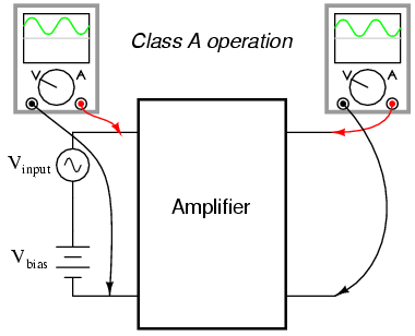
Class A operation is where the entire input waveform is faithfully reproduced. Although I didn't introduce this concept back in the common-emitter section, this is what we were hoping to attain in our simulations. Class A operation can only be obtained when the transistor spends its entire time in the active mode, never reaching either cutoff or saturation. To achieve this, sufficient DC bias voltage is usually set at the level necessary to drive the transistor exactly halfway between cutoff and saturation. This way, the AC input signal will be perfectly "centered" between the amplifier's high and low signal limit levels.
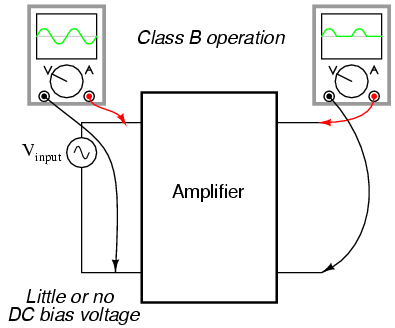
Class B operation is what we had the first time an AC signal was applied to the common-emitter amplifier with no DC bias voltage. The transistor spent half its time in active mode and the other half in cutoff with the input voltage too low (or even of the wrong polarity!) to forward-bias its base-emitter junction.
By itself, an amplifier operating in class B mode is not very useful. In most circumstances, the severe distortion introduced into the waveshape by eliminating half of it would be unacceptable. However, class B operation is a useful mode of biasing if two amplifiers are operated as a push-pull pair, each amplifier handling only half of the waveform at a time:
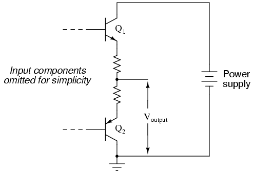
Transistor Q1 "pushes" (drives the output voltage in a positive direction with respect to ground), while transistor Q2 "pulls" the output voltage (in a negative direction, toward 0 volts with respect to ground). Individually, each of these transistors is operating in class B mode, active only for one-half of the input waveform cycle. Together, however, they function as a team to produce an output waveform identical in shape to the input waveform.
A decided advantage of the class B (push-pull) amplifier design over the class A design is greater output power capability. With a class A design, the transistor dissipates a lot of energy in the form of heat because it never stops conducting current. At all points in the wave cycle it is in the active (conducting) mode, conducting substantial current and dropping substantial voltage. This means there is substantial power dissipated by the transistor throughout the cycle. In a class B design, each transistor spends half the time in cutoff mode, where it dissipates zero power (zero current = zero power dissipation). This gives each transistor a time to "rest" and cool while the other transistor carries the burden of the load. Class A amplifiers are simpler in design, but tend to be limited to low-power signal applications for the simple reason of transistor heat dissipation.
There is another class of amplifier operation known as class AB, which is somewhere between class A and class B: the transistor spends more than 50% but less than 100% of the time conducting current.
If the input signal bias for an amplifier is slightly negative (opposite of the bias polarity for class A operation), the output waveform will be further "clipped" than it was with class B biasing, resulting in an operation where the transistor spends the majority of the time in cutoff mode:
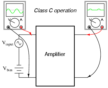
At first, this scheme may seem utterly pointless. After all, how useful could an amplifier be if it clips the waveform as badly as this? If the output is used directly with no conditioning of any kind, it would indeed be of questionable utility. However, with the application of a tank circuit (parallel resonant inductor-capacitor combination) to the output, the occasional output surge produced by the amplifier can set in motion a higher-frequency oscillation maintained by the tank circuit. This may be likened to a machine where a heavy flywheel is given an occasional "kick" to keep it spinning:
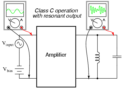
Called class C operation, this scheme also enjoys high power efficiency due to the fact that the transistor(s) spend the vast majority of time in the cutoff mode, where they dissipate zero power. The rate of output waveform decay (decreasing oscillation amplitude between "kicks" from the amplifier) is exaggerated here for the benefit of illustration. Because of the tuned tank circuit on the output, this type of circuit is usable only for amplifying signals of definite, fixed frequency.
Another type of amplifier operation, significantly different from Class A, B, AB, or C, is called Class D. It is not obtained by applying a specific measure of bias voltage as are the other classes of operation, but requires a radical re-design of the amplifier circuit itself. It's a little too early in this chapter to investigate exactly how a class D amplifier is built, but not too early to discuss its basic principle of operation.
A class D amplifier reproduces the profile of the input voltage waveform by generating a rapidly-pulsing squarewave output. The duty cycle of this output waveform (time "on" versus total cycle time) varies with the instantaneous amplitude of the input signal. The following plots demonstrate this principle:
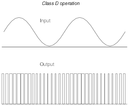
The greater the instantaneous voltage of the input signal, the greater the duty cycle of the output squarewave pulse. If there can be any goal stated of the class D design, it is to avoid active-mode transistor operation. Since the output transistor of a class D amplifier is never in the active mode, only cutoff or saturated, there will be little heat energy dissipated by it. This results in very high power efficiency for the amplifier. Of course, the disadvantage of this strategy is the overwhelming presence of harmonics on the output. Fortunately, since these harmonic frequencies are typically much greater than the frequency of the input signal, they can be filtered out by a low-pass filter with relative ease, resulting in an output more closely resembling the original input signal waveform. Class D technology is typically seen where extremely high power levels and relatively low frequencies are encountered, such as in industrial inverters (devices converting DC into AC power to run motors and other large devices) and high-performance audio amplifiers.
A term you will likely come across in your studies of electronics is something called quiescent, which is a modifier designating the normal, or zero input signal, condition of a circuit. Quiescent current, for example, is the amount of current in a circuit with zero input signal voltage applied. Bias voltage in a transistor circuit forces the transistor to operate at a different level of collector current with zero input signal voltage than it would without that bias voltage. Therefore, the amount of bias in an amplifier circuit determines its quiescent values.
In a class A amplifier, the quiescent current should be exactly half of its saturation value (halfway between saturation and cutoff, cutoff by definition being zero). Class B and class C amplifiers have quiescent current values of zero, since they are supposed to be cutoff with no signal applied. Class AB amplifiers have very low quiescent current values, just above cutoff. To illustrate this graphically, a "load line" is sometimes plotted over a transistor's characteristic curves to illustrate its range of operation while connected to a load resistance of specific value:
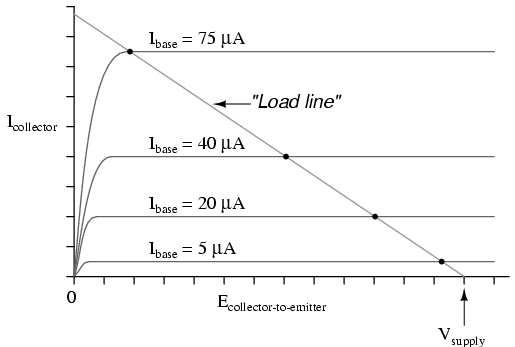
A load line is a plot of collector-to-emitter voltage over a range of base currents. At the lower-right corner of the load line, voltage is at maximum and current is at zero, representing a condition of cutoff. At the upper-left corner of the line, voltage is at zero while current is at a maximum, representing a condition of saturation. Dots marking where the load line intersects the various transistor curves represent realistic operating conditions for those base currents given.
Quiescent operating conditions may be shown on this type of graph in the form of a single dot along the load line. For a class A amplifier, the quiescent point will be in the middle of the load line, like this:
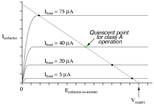
In this illustration, the quiescent point happens to fall on the curve representing a base current of 40 µA. If we were to change the load resistance in this circuit to a greater value, it would affect the slope of the load line, since a greater load resistance would limit the maximum collector current at saturation, but would not change the collector-emitter voltage at cutoff. Graphically, the result is a load line with a different upper-left point and the same lower-right point:
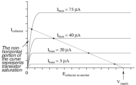
Note how the new load line doesn't intercept the 75 µA curve along its flat portion as before. This is very important to realize because the non-horizontal portion of a characteristic curve represents a condition of saturation. Having the load line intercept the 75 µA curve outside of the curve's horizontal range means that the amplifier will be saturated at that amount of base current. Increasing the load resistor value is what caused the load line to intercept the 75 µA curve at this new point, and it indicates that saturation will occur at a lesser value of base current than before.
With the old, lower-value load resistor in the circuit, a base current of 75 µA would yield a proportional collector current (base current multiplied by β). In the first load line graph, a base current of 75 µA gave a collector current almost twice what was obtained at 40 µA, as the β ratio would predict. Now, however, there is only a marginal increase in collector current between base current values of 75 µA and 40 µA, because the transistor begins to lose sufficient collector-emitter voltage to continue to regulate collector current.
In order to maintain linear (no-distortion) operation, transistor amplifiers shouldn't be operated at points where the transistor will saturate; that is, in any case where the load line will not potentially fall on the horizontal portion of a collector current curve. In this case, we'd have to add a few more curves to the graph before we could tell just how far we could "push" this transistor with increased base currents before it saturates.
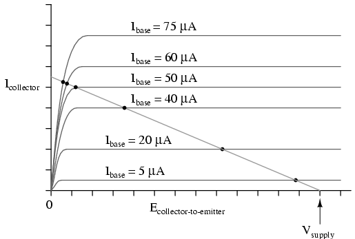
It appears in this graph that the highest-current point on the load line falling on the straight portion of a curve is the point on the 50 µA curve. This new point should be considered the maximum allowable input signal level for class A operation. Also for class A operation, the bias should be set so that the quiescent point is halfway between this new maximum point and cutoff:
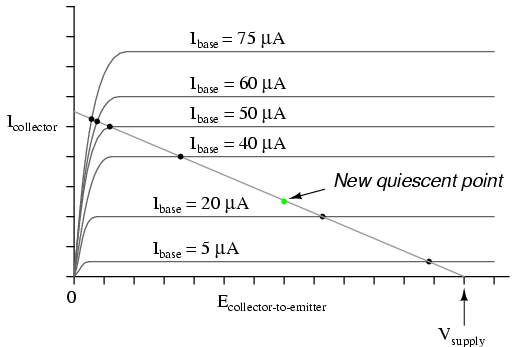
Now that we know a little more about the consequences of different DC bias voltage levels, it is time to investigate practical biasing techniques. So far, I've shown a small DC voltage source (battery) connected in series with the AC input signal to bias the amplifier for whatever desired class of operation. In real life, the connection of a precisely-calibrated battery to the input of an amplifier is simply not practical. Even if it were possible to customize a battery to produce just the right amount of voltage for any given bias requirement, that battery would not remain at its manufactured voltage indefinitely. Once it started to discharge and its output voltage drooped, the amplifier would begin to drift in the direction of class B operation.
Take this circuit, illustrated in the common-emitter section for a SPICE simulation, for instance:
That 2.3 volt "Vbias" battery would not be practical to include in a real amplifier circuit. A far more practical method of obtaining bias voltage for this amplifier would be to develop the necessary 2.3 volts using a voltage divider network connected across the 15 volt battery. After all, the 15 volt battery is already there by necessity, and voltage divider circuits are very easy to design and build. Let's see how this might look:
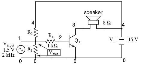
If we choose a pair of resistor values for R2 and R3 that will produce 2.3 volts across R3 from a total of 15 volts (such as 8466 Ω for R2 and 1533 Ω for R3), we should have our desired value of 2.3 volts between base and emitter for biasing with no signal input. The only problem is, this circuit configuration places the AC input signal source directly in parallel with R3 of our voltage divider. This is not acceptable, as the AC source will tend to overpower any DC voltage dropped across R3. Parallel components must have the same voltage, so if an AC voltage source is directly connected across one resistor of a DC voltage divider, the AC source will "win" and there will be no DC bias voltage added to the signal.
One way to make this scheme work, although it may not be obvious why it will work, is to place a coupling capacitor between the AC voltage source and the voltage divider like this:
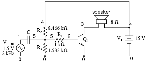
The capacitor forms a high-pass filter between the AC source and the DC voltage divider, passing almost all of the AC signal voltage on to the transistor while blocking all DC voltage from being shorted through the AC signal source. This makes much more sense if you understand the superposition theorem and how it works. According to superposition, any linear, bilateral circuit can be analyzed in a piecemeal fashion by only considering one power source at a time, then algebraically adding the effects of all power sources to find the final result. If we were to separate the capacitor and R2--R3 voltage divider circuit from the rest of the amplifier, it might be easier to understand how this superposition of AC and DC would work.
With only the AC signal source in effect, and a capacitor with an arbitrarily low impedance at signal frequency, almost all the AC voltage appears across R3:
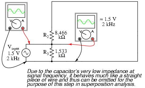
With only the DC source in effect, the capacitor appears to be an open circuit, and thus neither it nor the shorted AC signal source will have any effect on the operation of the R2--R3 voltage divider:
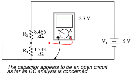
Combining these two separate analyses, we get a superposition of (almost) 1.5 volts AC and 2.3 volts DC, ready to be connected to the base of the transistor:
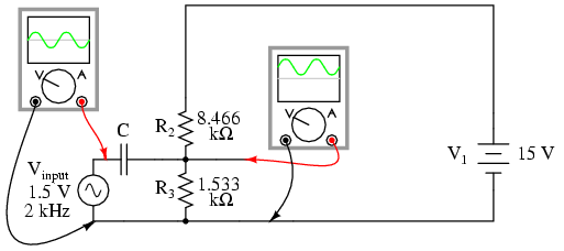
Enough talk -- it's about time for a SPICE simulation of the whole amplifier circuit. I'll use a capacitor value of 100 µF to obtain an arbitrarily low (0.796 Ω) impedance at 2000 Hz:
voltage divider biasing
vinput 1 0 sin (0 1.5 2000 0 0)
c1 1 5 100u
r1 5 2 1k
r2 4 5 8466
r3 5 0 1533
q1 3 2 0 mod1
rspkr 3 4 8
v1 4 0 dc 15
.model mod1 npn
.tran 0.02m 0.78m
.plot tran v(1,0) i(v1)
.end
legend:
*: v(1)
+: i(v1)
v(1)
(*)-- -2.000E+00   -1.000E+00    0.000E+00    1.000E+00   2.000E+00
(+)-- -3.000E-01   -2.000E-01   -1.000E-01    0.000E+00   1.000E-01
- - - - - - - - - - - - - - - - - - - - - - - - - - - - - - - - -
0.000E+00  .            .             *    +        .            .
3.730E-01  .            .             +    *        .            .
7.197E-01  .            .        +    .         *   .            .
1.022E+00  .            .    +        .             *            .
1.263E+00  .            . +           .             .   *        .
1.423E+00  .            +             .             .     *      .
1.490E+00  .           +.             .             .      *     .
1.467E+00  .           +.             .             .      *     .
1.357E+00  .            .+            .             .    *       .
1.152E+00  .            .  +          .             . *          .
8.774E-01  .            .      +      .           * .            .
5.505E-01  .            .           + .       *     .            .
1.878E-01  .            .             .  x          .            .
-1.870E-01 .            .          *  .       +     .            .
-5.500E-01 .            .     *       .           + .            .
-8.810E-01 .            . *           .             +            .
-1.152E+00 .          * .             .             +            .
-1.351E+00 .       *    .             .             +            .
-1.469E+00 .     *      .             .             +            .
-1.495E+00 .     *      .             .             +            .
-1.420E+00 .      *     .             .             +            .
-1.261E+00 .        *   .             .             +            .
-1.025E+00 .            *             .             +            .
-7.205E-01 .            .   *         .            +.            .
-3.713E-01 .            .        *    .         +   .            .
1.800E-04  .            .             *    +        .            .
3.726E-01  .            .             +    *        .            .
7.194E-01  .            .        +    .         *   .            .
1.022E+00  .            .    +        .             *            .
1.264E+00  .            . +           .             .   *        .
1.422E+00  .            +             .             .     *      .
1.490E+00  .           +.             .             .      *     .
1.468E+00  .           +.             .             .      *     .
1.357E+00  .            .+            .             .    *       .
1.151E+00  .            .  +          .             . *          .
8.775E-01  .            .      +      .           * .            .
5.509E-01  .            .           + .       *     .            .
1.877E-01  .            .             .  x          .            .
-1.871E-01 .            .          *  .       +     .            .
-5.522E-01 .            .     *       .           + .            .
- - - - - - - - - - - - - - - - - - - - - - - - - - - - - - - - -
Notice that there is substantial distortion in the output waveform here: the sine wave is being clipped during most of the input signal's negative half-cycle. This tells us the transistor is entering into cutoff mode when it shouldn't (I'm assuming a goal of class A operation as before). Why is this? This new biasing technique should give us exactly the same amount of DC bias voltage as before, right?
With the capacitor and R2--R3 resistor network unloaded, it will provide exactly 2.3 volts worth of DC bias. However, once we connect this network to the transistor, it is no longer loaded. Current drawn through the base of the transistor will load the voltage divider, thus reducing the DC bias voltage available for the transistor. Using the diode-regulating diode transistor model to illustrate, the bias problem becomes evident:
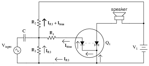
A voltage divider's output depends not only on the size of its constituent resistors, but also on how much current is being divided away from it through a load. In this case, the base-emitter PN junction of the transistor is a load that decreases the DC voltage dropped across R3, due to the fact that the bias current joins with R3's current to go through R2, upsetting the divider ratio formerly set by the resistance values of R2 and R3. In order to obtain a DC bias voltage of 2.3 volts, the values of R2 and/or R3 must be adjusted to compensate for the effect of base current loading. In this case, we want to increase the DC voltage dropped across R3, so we can lower the value of R2, raise the value of R3, or both.
voltage divider biasing
vinput 1 0 sin (0 1.5 2000 0 0)
c1 1 5 100u
r1 5 2 1k
r2 4 5 6k      <--- R2 decreased to 6 k ohms
r3 5 0 4k      <--- R3 increased to 4 k ohms
q1 3 2 0 mod1
rspkr 3 4 8
v1 4 0 dc 15
.model mod1 npn
.tran 0.02m 0.78m
.plot tran v(1,0) i(v1)
.end
legend:
*: v(1)
+: i(v1)
v(1)
(*)-- -2.000E+00   -1.000E+00    0.000E+00     1.000E+00  2.000E+00
(+)-- -3.000E-01   -2.000E-01   -1.000E-01     0.000E+00  1.000E-01
- - - - - - - - - - - - - - - - - - - - - - - - - - - - - - - - -
0.000E+00  .             .      +      *             .           .
3.730E-01  .             . +           .    *        .           .
7.197E-01  .          +  .             .         *   .           .
1.022E+00  .      +      .             .             *           .
1.263E+00  .  +          .             .             .   *       .
1.423E+00  .+            .             .             .     *     .
1.490E+00  +             .             .             .      *    .
1.467E+00  +             .             .             .      *    .
1.357E+00  . +           .             .             .    *      .
1.152E+00  .    +        .             .             . *         .
8.774E-01  .        +    .             .           * .           .
5.505E-01  .            +.             .       *     .           .
1.878E-01  .             .   +         .  *          .           .
-1.870E-01 .             .        + *  .             .           .
-5.500E-01 .             .     *       +             .           .
-8.810E-01 .             . *           .    +        .           .
-1.152E+00 .           * .             .       +     .           .
-1.351E+00 .        *    .             .          +  .           .
-1.469E+00 .      *      .             .           + .           .
-1.495E+00 .      *      .             .            +.           .
-1.420E+00 .       *     .             .           + .           .
-1.261E+00 .         *   .             .         +   .           .
-1.025E+00 .             *             .      +      .           .
-7.205E-01 .             .   *         .  +          .           .
-3.713E-01 .             .        *  + .             .           .
1.800E-04  .             .      +      *             .           .
3.726E-01  .             . +           .    *        .           .
7.194E-01  .          +  .             .         *   .           .
1.022E+00  .      +      .             .             *           .
1.264E+00  .  +          .             .             .   *       .
1.422E+00  .+            .             .             .     *     .
1.490E+00  +             .             .             .      *    .
1.468E+00  +             .             .             .      *    .
1.357E+00  . +           .             .             .    *      .
1.151E+00  .    +        .             .             . *         .
8.775E-01  .        +    .             .           * .           .
5.509E-01  .            +.             .       *     .           .
1.877E-01  .             .   +         .  *          .           .
-1.871E-01 .             .        + *  .             .           .
-5.522E-01 .             .     *       +             .           .
- - - - - - - - - - - - - - - - - - - - - - - - - - - - - - - - -
As you can see, the new resistor values of 6 kΩ and 4 kΩ (R2 and R3, respectively) results in class A waveform reproduction, just the way we wanted.
To overcome the challenge of creating necessary DC bias voltage for an amplifier's input signal without resorting to the insertion of a battery in series with the AC signal source, we used a voltage divider connected across the DC power source. To make this work in conjunction with an AC input signal, we "coupled" the signal source to the divider through a capacitor, which acted as a high-pass filter. With that filtering in place, the low impedance of the AC signal source couldn't "short out" the DC voltage dropped across the bottom resistor of the voltage divider. A simple solution, but not without any disadvantages.
Most obvious is the fact that using a high-pass filter capacitor to couple the signal source to the amplifier means that the amplifier can only amplify AC signals. A steady, DC voltage applied to the input would be blocked by the coupling capacitor just as much as the voltage divider bias voltage is blocked from the input source. Furthermore, since capacitive reactance is frequency-dependent, lower-frequency AC signals will not be amplified as much as higher-frequency signals. Non-sinusoidal signals will tend to be distorted, as the capacitor responds differently to each of the signal's constituent harmonics. An extreme example of this would be a low-frequency square-wave signal:
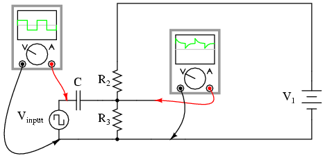
Incidentally, this same problem occurs when oscilloscope inputs are set to the "AC coupling" mode. In this mode, a coupling capacitor is inserted in series with the measured voltage signal to eliminate any vertical offset of the displayed waveform due to DC voltage combined with the signal. This works fine when the AC component of the measured signal is of a fairly high frequency, and the capacitor offers little impedance to the signal. However, if the signal is of a low frequency, and/or contains considerable levels of harmonics over a wide frequency range, the oscilloscope's display of the waveform will not be accurate.
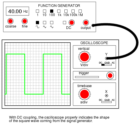
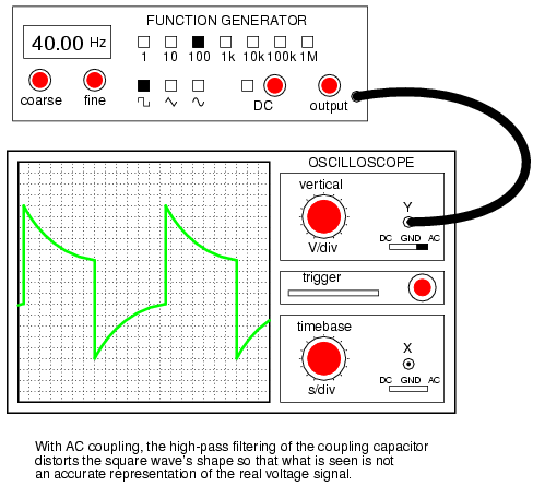
In applications where the limitations of capacitive coupling would be intolerable, another solution may be used: direct coupling. Direct coupling avoids the use of capacitors or any other frequency-dependent coupling component in favor of resistors. A direct-coupled amplifier circuit might look something like this:
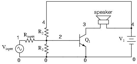
With no capacitor to filter the input signal, this form of coupling exhibits no frequency dependence. DC and AC signals alike will be amplified by the transistor with the same gain (the transistor itself may tend to amplify some frequencies better than others, but that is another subject entirely!).
If direct coupling works for DC as well as for AC signals, then why use capacitive coupling for any application? One reason might be to avoid any unwanted DC bias voltage naturally present in the signal to be amplified. Some AC signals may be superimposed on an uncontrolled DC voltage right from the source, and an uncontrolled DC voltage would make reliable transistor biasing impossible. The high-pass filtering offered by a coupling capacitor would work well here to avoid biasing problems.
Another reason to use capacitive coupling rather than direct is its relative lack of signal attenuation. Direct coupling through a resistor has the disadvantage of diminishing, or attenuating, the input signal so that only a fraction of it reaches the base of the transistor. In many applications, some attenuation is necessary anyway to prevent normal signal levels from "overdriving" the transistor into cutoff and saturation, so any attenuation inherent to the coupling network is useful anyway. However, some applications require that there be no signal loss from the input connection to the transistor's base for maximum voltage gain, and a direct coupling scheme with a voltage divider for bias simply won't suffice.
So far, we've discussed a couple of methods for coupling an input signal to an amplifier, but haven't addressed the issue of coupling an amplifier's output to a load. The example circuit used to illustrate input coupling will serve well to illustrate the issues involved with output coupling.
In our example circuit, the load is a speaker. Most speakers are electromagnetic in design: that is, they use the force generated by an lightweight electromagnet coil suspended within a strong permanent-magnet field to move a thin paper or plastic cone, producing vibrations in the air which our ears interpret as sound. An applied voltage of one polarity moves the cone outward, while a voltage of the opposite polarity will move the cone inward. To exploit cone's full freedom of motion, the speaker must receive true (unbiased) AC voltage. DC bias applied to the speaker coil tends to offset the cone from its natural center position, and this tends to limit the amount of back-and-forth motion it can sustain from the applied AC voltage without overtraveling. However, our example circuit applies a varying voltage of only one polarity across the speaker, because the speaker is connected in series with the transistor which can only conduct current one way. This situation would be unacceptable in the case of any high-power audio amplifier.
Somehow we need to isolate the speaker from the DC bias of the collector current so that it only receives AC voltage. One way to achieve this goal is to couple the transistor collector circuit to the speaker through a transformer:
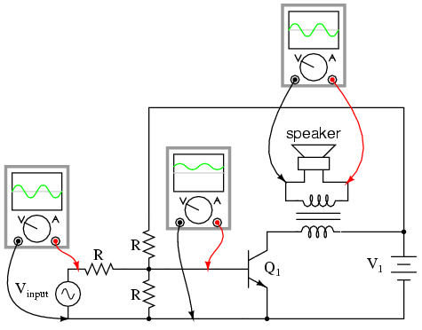
Voltage induced in the secondary (speaker-side) of the transformer will be strictly due to variations in collector current, because the mutual inductance of a transformer only works on changes in winding current. In other words, only the AC portion of the collector current signal will be coupled to the secondary side for powering the speaker. The speaker will "see" true alternating current at its terminals, without any DC bias.
Transformer output coupling works, and has the added benefit of being able to provide impedance matching between the transistor circuit and the speaker coil with custom winding ratios. However, transformers tend to be large and heavy, especially for high-power applications. Also, it is difficult to engineer a transformer to handle signals over a wide range of frequencies, which is almost always required for audio applications. To make matters worse, DC current through the primary winding adds to the magnetization of the core in one polarity only, which tends to make the transformer core saturate more easily in one AC polarity cycle than the other. This problem is reminiscent of having the speaker directly connected in series with the transistor: a DC bias current tends to limit how much output signal amplitude the system can handle without distortion. Generally, though, a transformer can be designed to handle a lot more DC bias current than a speaker without running into trouble, so transformer coupling is still a viable solution in most cases.
Another method to isolate the speaker from DC bias in the output signal is to alter the circuit a bit and use a coupling capacitor in a manner similar to coupling the input signal to the amplifier:
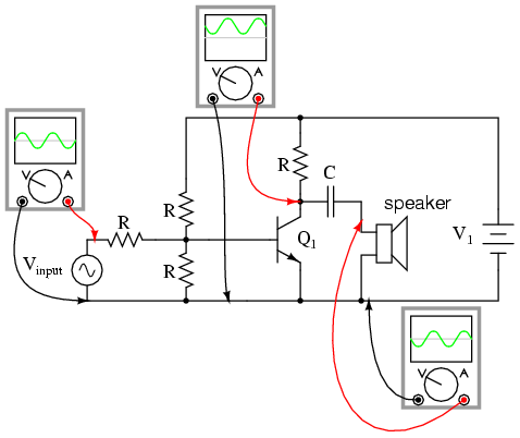
This circuit resembles the more conventional form of common-emitter amplifier, with the transistor collector connected to the battery through a resistor. The capacitor acts as a high-pass filter, passing most of the AC voltage to the speaker while blocking all DC voltage. Again, the value of this coupling capacitor is chosen so that its impedance at the expected signal frequency will be arbitrarily low.
The blocking of DC voltage from an amplifier's output, be it via a transformer or a capacitor, is useful not only in coupling an amplifier to a load, but also in coupling one amplifier to another amplifier. "Staged" amplifiers are often used to achieve higher power gains than what would be possible using a single transistor:
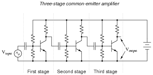
While it is possible to directly couple each stage to the next (via a resistor rather than a capacitor), this makes the whole amplifier very sensitive to variations in the DC bias voltage of the first stage, since that DC voltage will be amplified along with the AC signal until the last stage. In other words, the biasing of the first stage will affect the biasing of the second stage, and so on. However, if the stages are capacitively coupled as shown in the above illustration, the biasing of one stage has no effect on the biasing of the next, because DC voltage is blocked from passing on to the next stage.
Transformer coupling between amplifier stages is also a possibility, but less often seen due to some of the problems inherent to transformers mentioned previously. One notable exception to this rule is in the case of radio-frequency amplifiers where coupling transformers are typically small, have air cores (making them immune to saturation effects), and can be made part of a resonant circuit so as to block unwanted harmonic frequencies from passing on to subsequent stages. The use of resonant circuits assumes that the signal frequency remains constant, of course, but this is typically the case in radio circuitry. Also, the "flywheel" effect of LC tank circuits allows for class C operation for high efficiency:
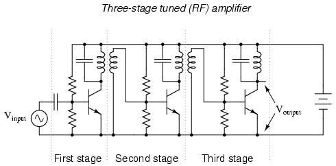
Having said all this, it must be mentioned that it is possible to use direct coupling within a multi-stage transistor amplifier circuit. In cases where the amplifier is expected to handle DC signals, this is the only alternative.
If some percentage of an amplifier's output signal is connected to the input, so that the amplifier amplifies part of its own output signal, we have what is known as feedback. Feedback comes in two varieties: positive (also called regenerative), and negative (also called degenerative). Positive feedback reinforces the direction of an amplifier's output voltage change, while negative feedback does just the opposite.
A familiar example of feedback happens in public-address ("PA") systems where someone holds the microphone too close to a speaker: a high-pitched "whine" or "howl" ensues, because the audio amplifier system is detecting and amplifying its own noise. Specifically, this is an example of positive or regenerative feedback, as any sound detected by the microphone is amplified and turned into a louder sound by the speaker, which is then detected by the microphone again, and so on . . . the result being a noise of steadily increasing volume until the system becomes "saturated" and cannot produce any more volume.
One might wonder what possible benefit feedback is to an amplifier circuit, given such an annoying example as PA system "howl." If we introduce positive, or regenerative, feedback into an amplifier circuit, it has the tendency of creating and sustaining oscillations, the frequency of which determined by the values of components handling the feedback signal from output to input. This is one way to make an oscillator circuit to produce AC from a DC power supply. Oscillators are very useful circuits, and so feedback has a definite, practical application for us.
Negative feedback, on the other hand, has a "dampening" effect on an amplifier: if the output signal happens to increase in magnitude, the feedback signal introduces a decreasing influence into the input of the amplifier, thus opposing the change in output signal. While positive feedback drives an amplifier circuit toward a point of instability (oscillations), negative feedback drives it the opposite direction: toward a point of stability.
An amplifier circuit equipped with some amount of negative feedback is not only more stable, but it tends to distort the input waveform to a lesser degree and is generally capable of amplifying a wider range of frequencies. The tradeoff for these advantages (there just has to be a disadvantage to negative feedback, right?) is decreased gain. If a portion of an amplifier's output signal is "fed back" to the input in such a way as to oppose any changes in the output, it will require a greater input signal amplitude to drive the amplifier's output to the same amplitude as before. This constitutes a decreased gain. However, the advantages of stability, lower distortion, and greater bandwidth are worth the tradeoff in reduced gain for many applications.
Let's examine a simple amplifier circuit and see how we might introduce negative feedback into it:
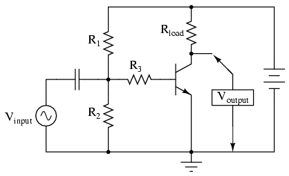
The amplifier configuration shown here is a common-emitter, with a resistor bias network formed by R1 and R2. The capacitor couples Vinput to the amplifier so that the signal source doesn't have a DC voltage imposed on it by the R1/R2 divider network. Resistor R3 serves the purpose of controlling voltage gain. We could omit if for maximum voltage gain, but since base resistors like this are common in common-emitter amplifier circuits, we'll keep it in this schematic.
Like all common-emitter amplifiers, this one inverts the input signal as it is amplified. In other words, a positive-going input voltage causes the output voltage to decrease, or go in the direction of negative, and visa-versa. If we were to examine the waveforms with oscilloscopes, it would look something like this:
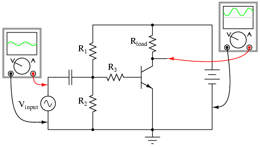
Because the output is an inverted, or mirror-image, reproduction of the input signal, any connection between the output (collector) wire and the input (base) wire of the transistor will result in negative feedback:
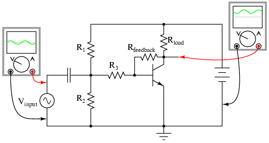
The resistances of R1, R2, R3, and Rfeedback function together as a signal-mixing network so that the voltage seen at the base of the transistor (in reference to ground) is a weighted average of the input voltage and the feedback voltage, resulting in signal of reduced amplitude going into the transistor. As a result, the amplifier circuit will have reduced voltage gain, but improved linearity (reduced distortion) and increased bandwidth.
A resistor connecting collector to base is not the only way to introduce negative feedback into this amplifier circuit, though. Another method, although more difficult to understand at first, involves the placement of a resistor between the transistor's emitter terminal and circuit ground, like this:
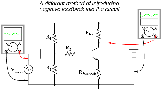
This new feedback resistor drops voltage proportional to the emitter current through the transistor, and it does so in such a way as to oppose the input signal's influence on the base-emitter junction of the transistor. Let's take a closer look at the emitter-base junction and see what difference this new resistor makes:
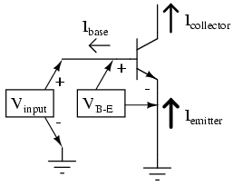
With no feedback resistor connecting the emitter to ground, whatever level of input signal (Vinput) makes it through the coupling capacitor and R1/R2/R3 resistor network will be impressed directly across the base-emitter junction as the transistor's input voltage (VB-E). In other words, with no feedback resistor, VB-E equals Vinput. Therefore, if Vinput increases by 100 mV, then VB-E likewise increases by 100 mV: a change in one is the same as a change in the other, since the two voltages are equal to each other.
Now let's consider the effects of inserting a resistor (Rfeedback) between the transistor's emitter lead and ground:
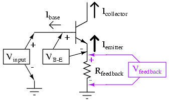
Note how the voltage dropped across Rfeedback adds with VB-E to equal Vinput. With Rfeedback in the Vinput -- VB-E loop, VB-E will no longer be equal to Vinput. We know that Rfeedback will drop a voltage proportional to emitter current, which is in turn controlled by the base current, which is in turn controlled by the voltage dropped across the base-emitter junction of the transistor (VB-E). Thus, if Vinput were to increase in a positive direction, it would increase VB-E, causing more base current, causing more collector (load) current, causing more emitter current, and causing more feedback voltage to be dropped across Rfeedback. This increase of voltage drop across the feedback resistor, though, subtracts from Vinput to reduce the VB-E, so that the actual voltage increase for VB-E will be less than the voltage increase of Vinput. No longer will a 100 mV increase in Vinput result in a full 100 mV increase for VB-E, because the two voltages are not equal to each other.
Consequently, the input voltage has less control over the transistor than before, and the voltage gain for the amplifier is reduced: just what we expected from negative feedback.
In practical common-emitter circuits, negative feedback isn't just a luxury; it's a necessity for stable operation. In a perfect world, we could build and operate a common-emitter transistor amplifier with no negative feedback, and have the full amplitude of Vinput impressed across the transistor's base-emitter junction. This would give us a large voltage gain. Unfortunately, though, the relationship between base-emitter voltage and base-emitter current changes with temperature, as predicted by the "diode equation." As the transistor heats up, there will be less of a forward voltage drop across the base-emitter junction for any given current. This causes a problem for us, as the R1/R2 voltage divider network is designed to provide the correct quiescent current through the base of the transistor so that it will operate in whatever class of operation we desire (in this example, I've shown the amplifier working in class-A mode). If the transistor's voltage/current relationship changes with temperature, the amount of DC bias voltage necessary for the desired class of operation will change. In this case, a hot transistor will draw more bias current for the same amount of bias voltage, making it heat up even more, drawing even more bias current. The result, if unchecked, is called thermal runaway.
Common-collector amplifiers, however, do not suffer from thermal runaway. Why is this? The answer has everything to do with negative feedback:
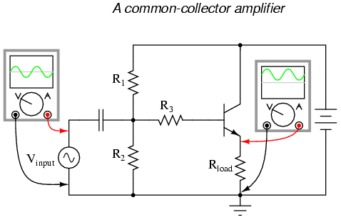
Note that the common-collector amplifier has its load resistor placed in exactly the same spot as we had the Rfeedback resistor in the last circuit: between emitter and ground. This means that the only voltage impressed across the transistor's base-emitter junction is the difference between Vinput and Voutput, resulting in a very low voltage gain (usually close to 1 for a common-collector amplifier). Thermal runaway is impossible for this amplifier: if base current happens to increase due to transistor heating, emitter current will likewise increase, dropping more voltage across the load, which in turn subtracts from Vinput to reduce the amount of voltage dropped between base and emitter. In other words, the negative feedback afforded by placement of the load resistor makes the problem of thermal runaway self-correcting. In exchange for a greatly reduced voltage gain, we get superb stability and immunity from thermal runaway.
By adding a "feedback" resistor between emitter and ground in a common-emitter amplifier, we make the amplifier behave a little less like an "ideal" common-emitter and a little more like a common-collector. The feedback resistor value is typically quite a bit less than the load, minimizing the amount of negative feedback and keeping the voltage gain fairly high.
Another benefit of negative feedback, seen clearly in the common-collector circuit, is that it tends to make the voltage gain of the amplifier less dependent on the characteristics of the transistor. Note that in a common-collector amplifier, voltage gain is nearly equal to unity (1), regardless of the transistor's β. This means, among other things, that we could replace the transistor in a common-collector amplifier with one having a different β and not see any significant changes in voltage gain. In a common-emitter circuit, the voltage gain is highly dependent on β. If we were to replace the transistor in a common-emitter circuit with another of differing β, the voltage gain for the amplifier would change significantly. In a common-emitter amplifier equipped with negative feedback, the voltage gain will still be dependent upon transistor β to some degree, but not as much as before, making the circuit more predictable despite variations in transistor β.
The fact that we have to introduce negative feedback into a common-emitter amplifier to avoid thermal runaway is an unsatisfying solution. It would be nice, after all, to avoid thermal runaway without having to suppress the amplifier's inherently high voltage gain. A best-of-both-worlds solution to this dilemma is available to us if we closely examine the nature of the problem: the voltage gain that we have to minimize in order to avoid thermal runaway is the DC voltage gain, not the AC voltage gain. After all, it isn't the AC input signal that fuels thermal runaway: it's the DC bias voltage required for a certain class of operation: that quiescent DC signal that we use to "trick" the transistor (fundamentally a DC device) into amplifying an AC signal. We can suppress DC voltage gain in a common-emitter amplifier circuit without suppressing AC voltage gain if we figure out a way to make the negative feedback function with DC only. That is, if we only feed back an inverted DC signal from output to input, but not an inverted AC signal.
The Rfeedback emitter resistor provides negative feedback by dropping a voltage proportional to load current. In other words, negative feedback is accomplished by inserting an impedance into the emitter current path. If we want to feed back DC but not AC, we need an impedance that is high for DC but low for AC. What kind of circuit presents a high impedance to DC but a low impedance to AC? A high-pass filter, of course!
By connecting a capacitor in parallel with the feedback resistor, we create the very situation we need: a path from emitter to ground that is easier for AC than it is for DC:
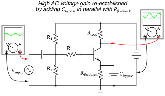
The new capacitor "bypasses" AC from the transistor's emitter to ground, so that no appreciable AC voltage will be dropped from emitter to ground to "feed back" to the input and suppress voltage gain. Direct current, on the other hand, cannot go through the bypass capacitor, and so must travel through the feedback resistor, dropping a DC voltage between emitter and ground which lowers the DC voltage gain and stabilizes the amplifier's DC response, preventing thermal runaway. Because we want the reactance of this capacitor (XC) to be as low as possible, Cbypass should be sized relatively large. Because the polarity across this capacitor will never change, it is safe to use a polarized (electrolytic) capacitor for the task.
Another approach to the problem of negative feedback reducing voltage gain is to use multi-stage amplifiers rather than single-transistor amplifiers. If the attenuated gain of a single transistor is insufficient for the task at hand, we can use more than one transistor to make up for the reduction caused by feedback. Here is an example circuit showing negative feedback in a three-stage common-emitter amplifier:
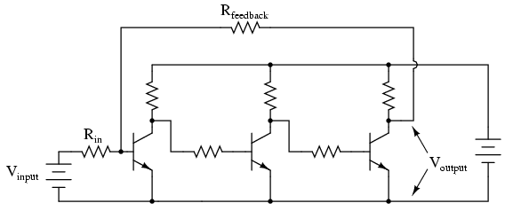
Note how there is but one "path" for feedback, from the final output to the input through a single resistor, Rfeedback. Since each stage is a common-emitter amplifier -- and thus inverting in nature -- and there are an odd number of stages from input to output, the output signal will be inverted with respect to the input signal, and the feedback will be negative (degenerative). Relatively large amounts of feedback may be used without sacrificing voltage gain, because the three amplifier stages provide so much gain to begin with.
At first, this design philosophy may seem inelegant and perhaps even counter-productive. Isn't this a rather crude way to overcome the loss in gain incurred through the use of negative feedback, to simply recover gain by adding stage after stage? What is the point of creating a huge voltage gain using three transistor stages if we're just going to attenuate all that gain anyway with negative feedback? The point, though perhaps not apparent at first, is increased predictability and stability from the circuit as a whole. If the three transistor stages are designed to provide an arbitrarily high voltage gain (in the tens of thousands, or greater) with no feedback, it will be found that the addition of negative feedback causes the overall voltage gain to become less dependent of the individual stage gains, and approximately equal to the simple ratio Rfeedback/Rin. The more voltage gain the circuit has (without feedback), the more closely the voltage gain will approximate Rfeedback/Rin once feedback is established. In other words, voltage gain in this circuit is fixed by the values of two resistors, and nothing more.
This advantage has profound impact on mass-production of electronic circuitry: if amplifiers of predictable gain may be constructed using transistors of widely varied β values, it makes the selection and replacement of components very easy and inexpensive. It also means the amplifier's gain varies little with changes in temperature. This principle of stable gain control through a high-gain amplifier "tamed" by negative feedback is elevated almost to an art form in electronic circuits called operational amplifiers, or op-amps. You may read much more about these circuits in a later chapter of this book!
*** PENDING ***
An interesting and often-used circuit applying the bipolar junction transistor is the so-called current mirror, which serves as a simple current regulator, supplying nearly constant current to a load over a wide range of load resistances.
We know that in a transistor operating in its active mode, collector current is equal to base current multiplied by the ratio β. We also know that the ratio between collector current and emitter current is called α. Because collector current is equal to base current multiplied by β, and emitter current is the sum of the base and collector currents, α should be mathematically derivable from β. If you do the algebra, you'll find that α = β/(β+1) for any transistor.
We've seen already how maintaining a constant base current through an active transistor results in the regulation of collector current, according to the β ratio. Well, the α ratio works similarly: if emitter current is held constant, collector current will remain at a stable, regulated value so long as the transistor has enough collector-to-emitter voltage drop to maintain it in its active mode. Therefore, if we have a way of holding emitter current constant through a transistor, the transistor will work to regulate collector current at a constant value.
Remember that the base-emitter junction of a BJT is nothing more than a PN junction, just like a diode, and that the "diode equation" specifies how much current will go through a PN junction given forward voltage drop and junction temperature:
If both junction voltage and temperature are held constant, then the PN junction current will likewise be constant. Following this rationale, if we were to hold the base-emitter voltage of a transistor constant, then its emitter current should likewise be constant, given a constant temperature:
This constant emitter current, multiplied by a constant α ratio, gives a constant collector current through Rload, provided that there is enough battery voltage to keep the transistor in its active mode for any change in Rload's resistance.
Maintaining a constant voltage across the transistor's base-emitter junction is easy: use a forward-biased diode to establish a constant voltage of approximately 0.7 volts, and connect it in parallel with the base-emitter junction:
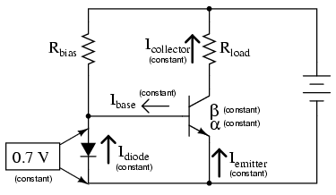
Now, here's where it gets interesting. The voltage dropped across the diode probably won't be 0.7 volts exactly. The exact amount of forward voltage dropped across it depends on the current through the diode, and the diode's temperature, all in accordance with the diode equation. If diode current is increased (say, by reducing the resistance of Rbias), its voltage drop will increase slightly, increasing the voltage drop across the transistor's base-emitter junction, which will increase the emitter current by the same proportion, assuming the diode's PN junction and the transistor's base-emitter junction are well-matched to each other. In other words, transistor emitter current will closely equal diode current at any given time. If you change the diode current by changing the resistance value of Rbias, then the transistor's emitter current will follow suit, because the emitter current is described by the same equation as the diode's, and both PN junctions experience the same voltage drop.
Remember, the transistor's collector current is almost equal to its emitter current, as the α ratio of a typical transistor is almost unity (1). If we have control over the transistor's emitter current by setting diode current with a simple resistor adjustment, then we likewise have control over the transistor's collector current. In other words, collector current mimics, or mirrors, diode current.
Current through resistor Rload is therefore a function of current set by the bias resistor, the two being nearly equal. This is the function of the current mirror circuit: to regulate current through the load resistor by conveniently adjusting the value of Rbias. It is very easy to create a set amount of diode current, as current through the diode is described by a simple equation: power supply voltage minus diode voltage (almost a constant value), divided by the resistance of Rbias.
To better match the characteristics of the two PN junctions (the diode junction and the transistor base-emitter junction), a transistor may be used in place of a regular diode, like this:
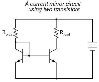
Because temperature is a factor in the "diode equation," and we want the two PN junctions to behave identically under all operating conditions, we should maintain the two transistors at exactly the same temperature. This is easily done using discrete components by gluing the two transistor cases back-to-back. If the transistors are manufactured together on a single chip of silicon (as a so-called integrated circuit, or IC), the designers should locate the two transistors very close to one another to facilitate heat transfer between them.
The current mirror circuit shown with two NPN transistors is sometimes called a current-sinking type, because the regulating transistor conducts current to the load from ground ("sinking" current), rather than from the positive side of the battery ("sourcing" current). If we wish to have a grounded load, and a current sourcing mirror circuit, we could use PNP transistors like this:
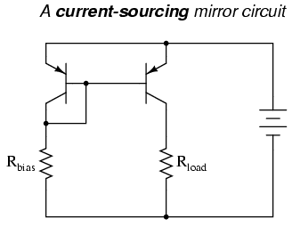
*** INCOMPLETE ***
Like all electrical and electronic components, transistors are limited in the amounts of voltage and current they can handle without sustaining damage. Since transistors are a bit more complex than some of the other components you're used to seeing at this point, they tend to have more kinds of ratings. What follows is an itemized description of some typical transistor ratings.
Power dissipation: When a transistor conducts current between collector and emitter, it also drops voltage between those two points. At any given time, the power dissipated by a transistor is equal to the product (multiplication) of collector current and collector-emitter voltage. Just like resistors, transistors are rated in terms of how many watts they can safely dissipate without sustaining damage. High temperature is the mortal enemy of all semiconductor devices, and bipolar transistors tend to be more susceptible to thermal damage than most. Power ratings are always given in reference to the temperature of ambient (surrounding) air. When transistors are to be used in hotter-than-normal environments, their power ratings must be derated to avoid a shortened service life.
Reverse voltages: As with diodes, bipolar transistors are rated for maximum allowable reverse-bias voltage across their PN junctions. This includes voltage ratings for the base-emitter junction, base-collector junction, and also from collector to emitter. The rating for maximum collector-emitter voltage can be thought of in terms of the maximum voltage it can withstand while in full-cutoff mode (no base current). This rating is of particular importance when using a bipolar transistor as a switch.
Collector current: A maximum value for collector current will be given by the manufacturer in amps. Understand that this maximum figure assumes a saturated state (minimum collector-emitter voltage drop). If the transistor is not saturated, and in fact is dropping substantial voltage between collector and emitter, the maximum power dissipation rating will probably be exceeded before the maximum collector current rating will. Just something to keep in mind when designing a transistor circuit!
Saturation voltages: Ideally, a saturated transistor acts as a closed switch contact between collector and emitter, dropping zero voltage at full collector current. In reality this is never true. Manufacturers will specify the maximum voltage drop of a transistor at saturation, both between the collector and emitter, and also between base and emitter (forward voltage drop of that PN junction). Collector-emitter voltage drop at saturation is generally expected to be 0.3 volts or less, but this figure is of course dependent on the specific type of transistor. Base-emitter forward voltage drop is very similar to that of an equivalent diode, which should come as no surprise.Beta: The ratio of collector current to base current, β is the fundamental parameter characterizing the amplifying ability of a bipolar transistor. β is usually assumed to be a constant figure in circuit calculations, but unfortunately this is far from true in practice. As such, manufacturers provide a set of β (or "hfe") figures for a given transistor over a wide range of operating conditions, usually in the form of maximum/minimum/typical ratings. It may surprise you to see just how widely β can be expected to vary within normal operating limits. One popular small-signal transistor, the 2N3903, is advertised as having a β ranging from 15 to 150 depending on the amount of collector current. Generally, β is highest for medium collector currents, decreasing for very low and very high collector currents.
Alpha: the ratio of collector current to emitter current, α may be derived from β, being equal to β/(β+1).
Bipolar transistors come in a wide variety of physical packages. Package type is primarily dependent upon the power dissipation of the transistor, much like resistors: the greater the maximum power dissipation, the larger the device has to be to stay cool. There are several standardized package types for three-terminal semiconductor devices, any of which may be used to house a bipolar transistor. This is an important fact to consider: there are many other semiconductor devices other than bipolar transistors which have three connection points. It is impossible to positively identify a three-terminal semiconductor device without referencing the part number printed on it, and/or subjecting it to a set of electrical tests.
*** PENDING ***
Nonlinearity Temperature drift Thermal runaway Junction capacitance Noise Mismatch (problem with paralleling transistors) β cutoff frequency Alpha cutoff frequencyLessons In Electric Circuits copyright (C) 2000-2003 Tony R. Kuphaldt, under the terms and conditions of the Design Science License.